 ChipApex | Global Electronic Components Supplier
SEARCH
Search Product
Search Post
— IC芯片 | 连接器 | 传感器 | 被动器件 —
Search productSearch post
— IC芯片 | 连接器 | 传感器 | 被动器件 —
Consult the customer manager about the wholesale price.
consultation hotline:86-132-6715-2157
email:[email protected]
Contact the product manager for consultation. One-stop consultation is available.
Do you want a lower wholesale price? Please send us your inquiry and we will reply immediately.
The LTC1064-4CJ is an obsolete 8th-order, clock-sweepable Cauer lowpass switched-capacitor filter housed in a 14-pin CERDIP package. It operates on dual power supplies ranging from ±2.37V to ±8V with a maximum total supply voltage of 16.5V. The device supports cutoff frequencies up to 100kHz using a 50:1 fCLK to fCUTOFF ratio, or up to 50kHz using a 100:1 transitional Butterworth-Cauer response. Key electrical specifications include a wideband noise of 135µVRMS at ±7.5V and a total harmonic distortion of 0.03% at 3VRMS input. The operating temperature range for the 'C' suffix is -40°C to +85°C.
Verify component authenticity carefully as this specific part number represents an obsolete package configuration. Confirm that the 14-lead CERDIP form factor remains compatible with existing board layouts before procurement. Ensure that any replacement strategy accounts for the discontinuation status by consulting current Analog Devices inventory for alternative sourcing options.
Select this component when a high-order analog filter response is required within a compact footprint. The external clock capability allows for precise tuning of the cutoff frequency relative to system timing references. Consider the transition between Cauer and Transitional modes based on the specific stopband attenuation requirements and delay linearity needs of the application design.
This device belongs to the LTC1064 family of low-noise, high-frequency switched-capacitor filters. It shares pin compatibility with the LTC1064-1, LTC1064-2, and LTC1064-3 variants, which offer different filter responses such as Elliptic, Butterworth, and Linear Phase. The 'CJ' designation specifically identifies the ceramic dual in-line package variant manufactured using the enhanced LTCMOS silicon gate process.
The datasheet explicitly lists the J Package as obsolete and recommends considering the N14 Package (PDIP) as an alternate source. Verify mechanical fitment if transitioning to the plastic DIP version.
Connecting Pin 10 to V+ establishes a 50:1 fCLK to fCUTOFF ratio for a Cauer response. Connecting Pin 10 to V– establishes a 100:1 fCLK to f–3dB ratio for a transitional Butterworth-Cauer response with lower noise and delay nonlinearity.
To achieve minimum passband ripple and cutoff frequencies above 20kHz, compensating components must be connected to the COMP1 and COMP2 pins. Specific values are required to maintain the ±0.1dB ripple specification at higher frequencies.
Bypassing Pin 10 with a 0.1µF capacitor reduces clock feedthrough. Additionally, buffering the output with a simple RC lowpass filter having a cutoff frequency of fCLK/3 can eliminate residual clock feedthrough artifacts.
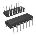 LTC1064-4CJ
The activity of extra discounts on wholesale prices is in full swing…
Please fill in your contact information and we will send you the latest wholesale price list.





