 ChipApex | Global Electronic Components Supplier
SEARCH
Search Product
Search Post
— IC芯片 | 连接器 | 传感器 | 被动器件 —
Search productSearch post
— IC芯片 | 连接器 | 传感器 | 被动器件 —
Consult the customer manager about the wholesale price.
consultation hotline:86-132-6715-2157
email:[email protected]
Contact the product manager for consultation. One-stop consultation is available.
Do you want a lower wholesale price? Please send us your inquiry and we will reply immediately.
The LTC1067IS#TRPBF is a dual, rail-to-rail, very low noise universal switched-capacitor building block. It integrates two identical second-order filter sections in a 16-lead SSOP package. The center frequency is tuned by an external clock with a nominal ratio of 100:1. Operating from a single 3V to –5V supply, it provides over 80dB dynamic range. Key electrical parameters include a typical power supply current of 4.5mA at 250kHz clock, a DC open-loop gain of 90dB, and a gain-bandwidth product of 2.8MHz. The device supports multiple operating modes for various filter topologies.
Verify the specific suffix TRPBF indicates tape and reel packaging when sourcing this component. Confirm the IS designation corresponds to the industrial temperature range specifications required for the intended application environment. Ensure the supplier provides valid traceability documentation consistent with Analog Devices manufacturing standards.
Select the LTC1067 variant over the LTC1067-50 if a higher clock-to-center frequency ratio is required for lower clock frequencies. Consider the thermal characteristics of the SSOP package for heat dissipation requirements. Evaluate the maximum Q versus center frequency graphs to ensure stability within the desired operating conditions and supply voltages.
This component belongs to the LTC1067 family of universal switched-capacitor filters. It shares architectural similarities with other Linear Technology precision analog building blocks but is specifically optimized for low-noise, high-dynamic-range filtering applications requiring precise frequency control via external clocks.
Public confirmed substitute part numbers are not available in the provided documentation. Designers should consult Analog Devices directly for potential cross-references or updated component recommendations.
The center frequency is determined by the external clock frequency applied to Pin 16. For the LTC1067, the nominal internal clock-to-center frequency ratio is fixed at 100:1, though this can be modified using external resistors in specific operating modes.
Any CMOS logic clock source with a square-wave output and a 50% duty cycle (±10%) is adequate. The clock source power supply should be isolated from the filter's power supply, and the analog ground should connect to the clock ground at a single point.
Yes, the device operates from a single supply ranging from 3V to 11V (with V– grounded) or dual supplies up to ±5V. In single-supply mode, the AGND pin must be bypassed to the analog ground plane with at least a 1µF capacitor.
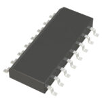 LTC1067IS#TRPBF
The activity of extra discounts on wholesale prices is in full swing…
Please fill in your contact information and we will send you the latest wholesale price list.





