ChipApex | Global Electronic Components Supplier

SEARCH
Search Product
Search Post
— IC芯片 | 连接器 | 传感器 | 被动器件 —
Search productSearch post
— IC芯片 | 连接器 | 传感器 | 被动器件 —
Consult the customer manager about the wholesale price.
consultation hotline:86-132-6715-2157
email:[email protected]
Contact the product manager for consultation. One-stop consultation is available.
Do you want a lower wholesale price? Please send us your inquiry and we will reply immediately.
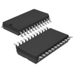
LTC1277CSW#TRPBF is listed in the Analog To Digital Converters (ADC) range at ChipApex. The manufacturer field lists Analog Devices Inc.. Its product description is IC ADC 12BIT SAR 24SOIC. Review the specifications below when checking this part for your BOM.
The Analog Devices LTC1277CSW#TRPBF is a 12-bit successive approximation analog-to-digital converter (ADC) housed in a 24-lead SO wide package. It operates from a single 5V or ±5V supply, consuming 10mW at a 100ksps sampling rate. The device features a differential input architecture and provides a two-byte read data format. Key electrical parameters include a typical signal-to-noise plus distortion ratio of 72dB at 100kHz input, total harmonic distortion of -82dB, and an internal 2.42V reference. Power management includes a Nap mode drawing 180µA and a Sleep mode reducing current to 1µA.
Verify the specific suffix #TRPBF indicates tape and reel packaging when sourcing. Confirm the CS variant meets commercial temperature requirements (0°C to 70°C). Ensure the logic supply voltage (VLOGIC) matches the host processor interface levels, as the LTC1277 supports both 3V and 5V logic interfaces via this pin.
Select the LTC1277 over the LTC1274 if a differential input is required for noise rejection. The LTC1277 offers distinct Nap and Sleep modes for flexible power management during inactive periods. Verify that the 2-byte read format aligns with the microprocessor's data bus access timing. Ensure the application can accommodate the 2µs acquisition time requirement for accurate signal settling.
The LTC1277 is part of the LTC1274/LTC1277 family of 12-bit, 10mW ADCs. While the LTC1274 utilizes a single-ended input and 12-bit parallel format, the LTC1277 distinguishes itself with a differential input structure and a two-byte readout mechanism. Both devices share identical power dissipation characteristics and sampling rates but differ in input topology and data interface.
Publicly confirmed substitute part numbers are not available in the provided documentation.
In bipolar mode, the LTC1277 accepts ±2.048V inputs and formats the digital output as offset binary.
The VLOGIC pin allows the user to select between a 3V or 5V logic interface, determining the voltage swing for all digital outputs including data bits, BUSY, and REFRDY.
Yes, the internal 2.42V reference can be overdriven positively by an external voltage source to adjust the input span range.
Explore related parts through Data Acquisition, Integrated Circuits (ICs), all product categories, ChipApex homepage.
 LTC1277CSW#TRPBF

The activity of extra discounts on wholesale prices is in full swing…
Please fill in your contact information and we will send you the latest wholesale price list.