 ChipApex | Global Electronic Components Supplier

SEARCH
Search Product
Search Post
— IC芯片 | 连接器 | 传感器 | 被动器件 —
Search productSearch post
— IC芯片 | 连接器 | 传感器 | 被动器件 —
Consult the customer manager about the wholesale price.
consultation hotline:86-132-6715-2157
email:[email protected]
Contact the product manager for consultation. One-stop consultation is available.
Do you want a lower wholesale price? Please send us your inquiry and we will reply immediately.
LTC1400CS8#TRPBF is listed in the Analog To Digital Converters (ADC) range at ChipApex. The manufacturer field lists Analog Devices Inc.. Its product description is IC ADC 12BIT SAR 8SOIC. Review the specifications below when checking this part for your BOM.
The LTC1400CS8#TRPBF is a complete 12-bit, 400ksps analog-to-digital converter in an 8-lead SOIC package. It operates from single 5V or ±5V supplies with typical power dissipation of 75mW at full speed. The device integrates a 200ns sample-and-hold circuit and a precision 2.42V internal reference. Key electrical specifications include ±1LSB INL/DNL, 72dB S/(N+D) at Nyquist, and a 3-wire serial interface compatible with DSPs. Power management features include Nap mode (6mW) for instant wake-up and Sleep mode (30μW).
Verify the #TRPBF suffix confirms tape and reel packaging and lead-free compliance. Confirm the 'C' grade designation matches the required 0°C to 70°C operating temperature range. Ensure the source document explicitly lists this part number as available from Analog Devices Inc. distributors.
Select this component for applications requiring moderate resolution (12-bit) at high speeds (400ksps) with low power constraints. Choose bipolar operation if negative input voltages are needed, utilizing the VSS pin. For unipolar applications, tie VSS to GND. Ensure the driving amplifier can settle within the 200ns acquisition time.
This part belongs to the LTC1400 family of complete ADCs. The CS8 variant denotes the commercial temperature range and SOIC-8 plastic package. The #TRPBF suffix indicates the specific ordering configuration for tape and reel supply with RoHS-compliant finishes.
Direct substitutes must maintain 12-bit resolution, 400ksps sampling rate, and SOIC-8 packaging. Verify pin compatibility for VCC, AIN, VREF, GND, DOUT, CLK, CONV, and VSS. Check that replacement devices support similar power modes and serial interface timing requirements.
The device automatically detects the mode based on the VSS pin voltage. If VSS is connected to GND, it operates in unipolar mode (0V to 4.096V). If VSS is connected to -5V, it switches to bipolar mode (±2.048V).
Upon waking from Sleep mode, the device requires approximately 4ms for the internal reference to settle. The REFREADY bit in the serial data word indicates when the reference is stable and conversion can begin.
Yes, the VREF pin can be driven externally by a DAC or precision reference to adjust the input span. The external voltage must be at least 2.45V to prevent conflict with the internal reference but should not exceed 5V.
Explore related parts through Data Acquisition, Integrated Circuits (ICs), all product categories, ChipApex homepage.
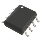 LTC1400CS8#TRPBF

The activity of extra discounts on wholesale prices is in full swing…
Please fill in your contact information and we will send you the latest wholesale price list.





