 ChipApex | Global Electronic Components Supplier

SEARCH
Search Product
Search Post
— IC芯片 | 连接器 | 传感器 | 被动器件 —
Search productSearch post
— IC芯片 | 连接器 | 传感器 | 被动器件 —
Consult the customer manager about the wholesale price.
consultation hotline:86-132-6715-2157
email:[email protected]
Contact the product manager for consultation. One-stop consultation is available.
Do you want a lower wholesale price? Please send us your inquiry and we will reply immediately.
LTC1402IGN#TRPBF is listed in the Analog To Digital Converters (ADC) range at ChipApex. The manufacturer field lists Analog Devices Inc.. Its product description is IC ADC 12BIT SAR 16SSOP. Review the specifications below when checking this part for your BOM.
The LTC1402IGN#TRPBF is a 12-bit, 2.2Msps sampling analog-to-digital converter (ADC) from Analog Devices Inc., housed in a 16-lead narrow SSOP package. It features a high dynamic range sample-and-hold circuit and an internal 4.096V reference. The device operates on a single 5V supply or dual ±5V supplies, consuming 90mW in active mode. Key performance metrics include 72dB S/(N+D) and –89dB THD at Nyquist. It supports unipolar (0V to 4.096V) and bipolar (–2.048V) input ranges via the BIP/UNI pin. Power management includes Nap (15mW) and Sleep (10mW) modes with instant wake-up capabilities.
Verify the specific suffix #TRPBF indicates tape and reel packaging when sourcing. Confirm the 'I' grade designation for the –40°C to 85°C industrial temperature range. Ensure compatibility with the required logic voltage levels (3V or 5V) for the OVDD pin before procurement.
Select this component for applications demanding high throughput and low power consumption. Use the Nap mode for frequent short bursts of activity to save energy while maintaining immediate readiness. Choose bipolar mode with dual supplies for optimal noise performance with op amps, or unipolar mode for single-supply simplicity.
This part belongs to the LTC1402 family of serial ADCs. The IGN#TRPBF designation specifies the Industrial temperature grade, Narrow SSOP package, and Tape & Reel packaging format. It is designed to replace older parallel ADCs in space-constrained designs due to its compact 16-pin footprint and serial interface.
When replacing legacy ADCs, ensure the new driver amplifier can settle within the 57ns acquisition time. Verify that the host processor's serial port timing matches the LTC1402's SCK and CONV requirements. Check if external reference buffering is needed if the internal VREF load exceeds specifications.
Tying BIP/UNI to logic high sets bipolar mode with a –2.048V range, optimized for dual supplies. Tying it to logic low sets unipolar mode with a 0V to 4.096V range, suitable for single-supply systems.
Nap mode consumes 15mW and allows immediate conversion upon receiving clock pulses. Sleep mode consumes 10mW but requires a 10ms wait for the internal reference to settle after waking up, indicated by the REFREADY bit.
Yes, the VREF pin can be driven by an external source or a DAC output. When using an external reference, the GAIN pin should be tied to VREF to set the full-scale range appropriately.
Explore related parts through Data Acquisition, Integrated Circuits (ICs), all product categories, ChipApex homepage.
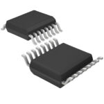 LTC1402IGN#TRPBF

The activity of extra discounts on wholesale prices is in full swing…
Please fill in your contact information and we will send you the latest wholesale price list.




