 ChipApex | Global Electronic Components Supplier

SEARCH
Search Product
Search Post
— IC芯片 | 连接器 | 传感器 | 被动器件 —
Search productSearch post
— IC芯片 | 连接器 | 传感器 | 被动器件 —
Consult the customer manager about the wholesale price.
consultation hotline:86-132-6715-2157
email:[email protected]
Contact the product manager for consultation. One-stop consultation is available.
Do you want a lower wholesale price? Please send us your inquiry and we will reply immediately.
LTC1404CS8#PBF is listed in the Analog To Digital Converters (ADC) range at ChipApex. The manufacturer field lists Analog Devices Inc.. Its product description is IC ADC 12BIT SAR 8SOIC. Review the specifications below when checking this part for your BOM.
The LTC1404CS8#PBF is a complete 12-bit, 600ksps sampling A/D converter in an SO-8 package. It operates from a single 5V supply or ±5V supplies, drawing 75mW at full speed. The device features a 160ns sample-and-hold and an internal 2.43V reference. It supports unipolar (0V to 4.096V) and bipolar (±2.048V) input ranges with guaranteed no missing codes. Key specifications include ±1LSB INL/DNL, 72dB S/(N+D), and –80dB THD at Nyquist. Power management includes Nap mode (7.5mW) and Sleep mode (60µW).
Verify the suffix #PBF indicates lead-free compliance. Confirm the CS8 variant specifies the commercial temperature range of 0°C to 70°C. Ensure the ordering code matches the required package style and pin configuration for the target PCB design.
Select this component for applications requiring high throughput up to 600ksps with minimal external components. Choose the IS8 variant if operation below 0°C is required. Consider the internal reference limitations when higher precision or wider input spans are needed compared to external references.
This part belongs to the LTC1404 family of monolithic sampling ADCs. The CS8 designation identifies the commercial grade version housed in an 8-lead plastic SOIC package. It serves as a compact solution for replacing discrete ADC designs in space-constrained electronics.
Direct replacements within the same family include the LTC1404IS8#PBF for extended temperature ranges. Verify pin compatibility and electrical specifications against legacy parts before substitution.
The device automatically detects the mode based on the VSS pin potential. If VSS is tied to GND, it operates in unipolar mode. If VSS is connected to a negative supply (e.g., -5V), it switches to bipolar mode.
Upon waking from Sleep mode, the device requires approximately 2.5ms for the internal reference to settle. The REFREADY bit in the serial data word indicates when the chip is ready to convert.
Yes, the 2.43V internal reference is available at Pin 3 (VREF). It can drive external loads up to 1mA or be overdriven by an external source to adjust input span, provided the voltage stays between 2.43V and 5V.
Explore related parts through Data Acquisition, Integrated Circuits (ICs), all product categories, ChipApex homepage.
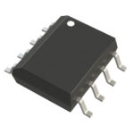 LTC1404CS8#PBF

The activity of extra discounts on wholesale prices is in full swing…
Please fill in your contact information and we will send you the latest wholesale price list.




