 ChipApex | Global Electronic Components Supplier

SEARCH
Search Product
Search Post
— IC芯片 | 连接器 | 传感器 | 被动器件 —
Search productSearch post
— IC芯片 | 连接器 | 传感器 | 被动器件 —
Consult the customer manager about the wholesale price.
consultation hotline:86-132-6715-2157
email:[email protected]
Contact the product manager for consultation. One-stop consultation is available.
Do you want a lower wholesale price? Please send us your inquiry and we will reply immediately.
LTC1406IGN#TRPBF is listed in the Analog To Digital Converters (ADC) range at ChipApex. The manufacturer field lists Analog Devices Inc.. Its product description is IC ADC 8BIT PIPELINED 24SSOP. Review the specifications below when checking this part for your BOM.
The LTC1406IGN#TRPBF is a low-power, 8-bit, 20Msps sampling A/D converter housed in a 24-lead narrow SSOP package. It operates from a single 5V supply with typical power dissipation of 150mW at full throughput. The device features a 250MHz internal sample-and-hold amplifier and true differential analog inputs (AIN+, AIN–) that reject common-mode noise. Key electrical specifications include ±1LSB maximum DNL and INL over temperature, a full-scale input span of ±1V, and an output data latency of five clock cycles. The part supports interface to 3V digital systems via separate OVDD and OGND pins.
Verify the ordering suffix #TRPBF indicates tape and reel packaging for the IGN industrial temperature grade variant. Confirm the component status is Active. Ensure compatibility with the required 24-lead narrow SSOP footprint during procurement planning.
Select this component for applications requiring high dynamic range at moderate speeds. The 250MHz bandwidth allows undersampling of signals well beyond the Nyquist frequency. Ensure the driving circuit has sufficient settling time (<25ns) to handle the sampling capacitor charge spikes at 20Msps throughput.
This part belongs to the LTC1406 family of sampling ADCs. The IGN suffix denotes the Industrial temperature range (-40°C to 85°C), distinguishing it from the CGN Commercial grade variant. The #TRPBF suffix specifies the Tape & Reel packaging format with lead-free finish.
The LTC1406CGN#TRPBF is a direct functional substitute within the same package and pinout, differing only in the commercial temperature range specification (0°C to 70°C).
For single-ended operation, tie the AIN– pin to a fixed DC voltage (such as VREF) and drive the AIN+ pin with the signal. The input span remains ±1V relative to the common mode.
The pipelined architecture introduces a latency of five clock cycles between the falling edge of the CLK input (which starts conversion) and the availability of valid data on the output pins.
Yes. The digital inputs accept 3V or 5V logic levels. The outputs can be powered by a separate OVDD supply as low as 2.7V to match 3V logic requirements.
Explore related parts through Data Acquisition, Integrated Circuits (ICs), all product categories, ChipApex homepage.
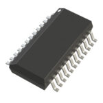 LTC1406IGN#TRPBF

The activity of extra discounts on wholesale prices is in full swing…
Please fill in your contact information and we will send you the latest wholesale price list.




