 ChipApex | Global Electronic Components Supplier

SEARCH
Search Product
Search Post
— IC芯片 | 连接器 | 传感器 | 被动器件 —
Search productSearch post
— IC芯片 | 连接器 | 传感器 | 被动器件 —
Consult the customer manager about the wholesale price.
consultation hotline:86-132-6715-2157
email:[email protected]
Contact the product manager for consultation. One-stop consultation is available.
Do you want a lower wholesale price? Please send us your inquiry and we will reply immediately.
LTC1411CG#PBF is listed in the Analog To Digital Converters (ADC) range at ChipApex. The manufacturer field lists Analog Devices Inc.. Its product description is IC ADC 14BIT SAR 36SSOP. Review the specifications below when checking this part for your BOM.
The LTC1411CG#PBF is a single-supply, 14-bit, 2.5Msps analog-to-digital converter housed in a 36-lead plastic SSOP package. It operates from a single 5V supply with typical power dissipation of 195mW. The device integrates a high-bandwidth sample-and-hold circuit, a precision internal reference, and an internally trimmed clock. It supports differential or single-ended inputs and provides four programmable input ranges selected via digital pins. Dynamic performance includes 80dB S/(N + D) and 90dB THD at a 100kHz input frequency.
Verify the operating temperature range matches the application requirements; the 'C' suffix indicates a commercial range of 0°C to 70°C. Confirm that the 36-lead SSOP package dimensions align with the PCB footprint. Ensure the design accommodates the specific bypass capacitor values required for the REFCOM1, REFCOM2, and AVP pins to maintain specified noise and linearity performance.
Select this component when a single 5V supply and moderate power consumption are required. The internal 2.5V reference may be sufficient for many applications, but external references can be used via the REFIN pin for improved drift characteristics. Consider the wake-up times: 210ms from Sleep mode and 250ns from Nap mode when designing power management sequences. The device outputs data in 2's complement format.
The LTC1411 is part of Analog Devices' family of high-speed successive approximation ADCs. The LTC1411CG#PBF specifically denotes the commercial temperature grade version packaged in a 36-lead SSOP. It serves as a bridge between analog signals and digital processing units, offering a balance between resolution, speed, and power efficiency for general-purpose high-performance data conversion tasks.
Public confirmed substitute part numbers are not available in the provided documentation.
The input ranges are selected using two digital logic inputs, PGA0 and PGA1. These pins control the internal DAC reference voltage (REFCOM2), providing spans of –1.8V, –1.27V, –0.9V, and –0.64V relative to the voltage applied to AIN–.
In Sleep mode, the ADC draws less than 1mA, but requires approximately 210ms to wake up due to the time needed for the REFCOM2 bypass capacitor to charge. In Nap mode, the ADC draws about 2mA while keeping the internal reference active, allowing for a much faster wake-up time of 250ns.
The OTR pin goes high when the analog input exceeds the selected input range. By combining the OTR signal with the Most Significant Bit (D13), one can distinguish between overrange (OTR high, D13 low) and underrange (OTR high, D13 high) conditions.
Explore related parts through Data Acquisition, Integrated Circuits (ICs), all product categories, ChipApex homepage.
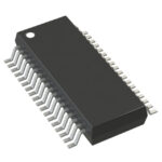 LTC1411CG#PBF

The activity of extra discounts on wholesale prices is in full swing…
Please fill in your contact information and we will send you the latest wholesale price list.




