 ChipApex | Global Electronic Components Supplier

SEARCH
Search Product
Search Post
— IC芯片 | 连接器 | 传感器 | 被动器件 —
Search productSearch post
— IC芯片 | 连接器 | 传感器 | 被动器件 —
Consult the customer manager about the wholesale price.
consultation hotline:86-132-6715-2157
email:[email protected]
Contact the product manager for consultation. One-stop consultation is available.
Do you want a lower wholesale price? Please send us your inquiry and we will reply immediately.
LTC1411CG#TRPBF is listed in the Analog To Digital Converters (ADC) range at ChipApex. The manufacturer field lists Analog Devices Inc.. Its product description is IC ADC 14BIT SAR 36SSOP. Review the specifications below when checking this part for your BOM.
The LTC1411CG#TRPBF is a single-supply, 14-bit, 2.5Msps analog-to-digital converter housed in a 36-lead SSOP package. It operates from a single 5V supply with typical power dissipation of 195mW. The device integrates a high-bandwidth sample-and-hold circuit, a precision internal reference, and an internally trimmed clock. It supports differential or single-ended inputs and provides four programmable input ranges selected via digital pins. Key performance metrics include –2LSB integral nonlinearity, 80dB S/(N + D), and 90dB THD at a 100kHz input frequency.
Verify the specific suffix #TRPBF indicates tape and reel packaging when sourcing components. Confirm that the CG variant meets the required commercial operating temperature range of 0°C to 70°C. Ensure compatibility with standard 36-lead SSOP footprints during procurement planning.
Select this component for applications requiring high dynamic performance at moderate speeds. The 14-bit resolution and low distortion make it suitable for precision measurement tasks. Consider the available programmable input ranges to match signal amplitudes without external attenuation. Evaluate power constraints against the 195mW typical dissipation or utilize Nap/Sleep modes for lower standby current.
This part belongs to the LTC1411 family of high-speed ADCs. The CG suffix denotes the commercial temperature grade (0°C to 70°C), while the IG suffix would indicate an industrial grade (-40°C to 85°C). The TRPBF suffix specifies the reel packaging format for automated assembly.
Direct replacements within the same family include the LTC1411IG#TRPBF for industrial temperature requirements. Other Analog Devices ADCs may require significant interface or performance adjustments due to differing architectures or pinouts.
The input ranges are selected using two digital logic inputs, PGA0 and PGA1. These pins control the internal reference voltage applied to the DAC, providing spans of –1.8V, –1.27V, –0.9V, and –0.64V relative to the AIN– pin.
When exiting Sleep mode, the ADC requires approximately 210ms to wake up if a 10µF bypass capacitor is used on the REFCOM2 pin. This allows the internal reference and compensation circuits to stabilize.
The LTC1411 features an Out-of-the-Range (OTR) digital output. Combined with the Most Significant Bit (D13), it indicates whether the analog input exceeds the maximum voltage (overrange) or falls below the minimum voltage (underrange) of the selected input range.
Explore related parts through Data Acquisition, Integrated Circuits (ICs), all product categories, ChipApex homepage.
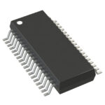 LTC1411CG#TRPBF

The activity of extra discounts on wholesale prices is in full swing…
Please fill in your contact information and we will send you the latest wholesale price list.




