 ChipApex | Global Electronic Components Supplier

SEARCH
Search Product
Search Post
— IC芯片 | 连接器 | 传感器 | 被动器件 —
Search productSearch post
— IC芯片 | 连接器 | 传感器 | 被动器件 —
Consult the customer manager about the wholesale price.
consultation hotline:86-132-6715-2157
email:[email protected]
Contact the product manager for consultation. One-stop consultation is available.
Do you want a lower wholesale price? Please send us your inquiry and we will reply immediately.
LTC1740CG#PBF is listed in the Analog To Digital Converters (ADC) range at ChipApex. The manufacturer field lists Analog Devices Inc.. Its product description is IC ADC 14BIT PIPELINED 36SSOP. Review the specifications below when checking this part for your BOM.
The LTC1740CG#PBF is a 14-bit, 6Msps sampling analog-to-digital converter (ADC) housed in a 36-lead SSOP package. It operates from a single 5V supply or dual ±5V supplies with a typical power dissipation of 245mW. The device features true differential inputs with 75dB CMRR and an internal programmable reference supporting input ranges of ±2.5V or ±1.25V. Key performance metrics include 79dB S/(N+D) and 91dB SFDR at a 2.5MHz input frequency. The part is rated for commercial temperatures ranging from 0°C to 70°C.
Verify the 'C' suffix indicates the commercial temperature range (0°C to 70°C). Confirm the '#PBF' designation ensures compliance with RoHS standards and absence of lead. Check current availability status as component lifecycle changes may affect stock levels.
Select this model when a 14-bit resolution and 6Msps throughput are required within a low-power budget of 245mW. Ensure the application can accommodate the 36-pin SSOP footprint. Verify that the system clock jitter remains below specifications to maintain the stated 79dB SNR performance.
This component belongs to the LTC1740 family of high-speed ADCs. The CG variant specifically denotes the commercial temperature grade. It serves as a complete solution integrating a sample-and-hold circuit, pipelined ADC core, and precision reference into a single compact package.
Consult manufacturer documentation for direct pin-compatible substitutes. Evaluate alternative ADCs based on matching resolution, sampling speed, and interface requirements if the LTC1740CG#PBF is unavailable.
The LTC1740 provides a parallel 14-bit two's complement binary output.
The input range is set by the VREF pin voltage, which can be internally generated as 4.5V (±2.5V range) or 2.25V (±1.25V range), or driven externally via the SENSE pin.
The conversion result appears at the outputs after three clock cycles following the rising edge of the CLK signal.
Explore related parts through Data Acquisition, Integrated Circuits (ICs), all product categories, ChipApex homepage.
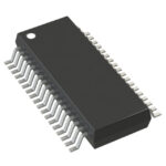 LTC1740CG#PBF

The activity of extra discounts on wholesale prices is in full swing…
Please fill in your contact information and we will send you the latest wholesale price list.




