 ChipApex | Global Electronic Components Supplier

SEARCH
Search Product
Search Post
— IC芯片 | 连接器 | 传感器 | 被动器件 —
Search productSearch post
— IC芯片 | 连接器 | 传感器 | 被动器件 —
Consult the customer manager about the wholesale price.
consultation hotline:86-132-6715-2157
email:[email protected]
Contact the product manager for consultation. One-stop consultation is available.
Do you want a lower wholesale price? Please send us your inquiry and we will reply immediately.
LTC1749CFW#TRPBF is listed in the Analog To Digital Converters (ADC) range at ChipApex. The manufacturer field lists Analog Devices Inc.. Its product description is IC ADC 12BIT PIPELINED 48TSSOP. Review the specifications below when checking this part for your BOM.
The LTC1749CFW#TRPBF is a high-speed, 12-bit analog-to-digital converter (ADC) from Analog Devices Inc., housed in a 48-lead TSSOP package. It operates at a sampling rate of 80Msps with a full power bandwidth of 500MHz. The device features an integrated programmable gain amplifier (PGA) and sample-and-hold circuit, supporting differential input ranges of 2.25Vp-p or 1.35Vp-p. Key performance metrics include a signal-to-noise ratio (SNR) of 71.8dB and spurious-free dynamic range (SFDR) of 87dB at 5MHz input. It requires a single 5V supply and dissipates approximately 1.45W.
Verify the specific suffix 'CFW#TRPBF' against official Analog Devices documentation to confirm the temperature grade (Commercial, 0°C to 70°C), package type (TSSOP-48), and tape-and-reel packaging configuration. Ensure compatibility with system voltage requirements and thermal management needs given the 1.45W power dissipation.
Select this component when digitizing wide dynamic range signals up to 500MHz is required. The internal PGA allows optimization of the input range without external amplifiers. Consider the 5-cycle data latency and the requirement for differential encoding inputs (ENC/ENC) when designing the digital interface timing.
This part belongs to the LTC1749 family of wide-bandwidth ADCs. It is pin-compatible with the 14-bit 80Msps LTC1750, allowing for design flexibility between resolution and speed requirements within the same footprint.
The LTC1749CFW#PBF is listed as a parameter-equivalent alternative in distributor databases. Verify if the non-trailing 'PBF' suffix denotes a tube package instead of tape-and-reel, which may impact assembly processes.
The LTC1749 supports a full power bandwidth of 500MHz, allowing it to digitize wide dynamic range signals up to this frequency.
The Programmable Gain Amplifier (PGA) allows selection between an effective front-end gain of 1 (2.25Vp-p input range) and 1 2/3 (1.35Vp-p input range).
Yes, the MSBINV pin controls the output format. A low state selects 2's complement format, while a high state selects offset binary format.
Explore related parts through Data Acquisition, Integrated Circuits (ICs), all product categories, ChipApex homepage.
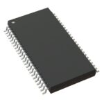 LTC1749CFW#TRPBF

The activity of extra discounts on wholesale prices is in full swing…
Please fill in your contact information and we will send you the latest wholesale price list.





