 ChipApex | Global Electronic Components Supplier

SEARCH
Search Product
Search Post
— IC芯片 | 连接器 | 传感器 | 被动器件 —
Search productSearch post
— IC芯片 | 连接器 | 传感器 | 被动器件 —
Consult the customer manager about the wholesale price.
consultation hotline:86-132-6715-2157
email:[email protected]
Contact the product manager for consultation. One-stop consultation is available.
Do you want a lower wholesale price? Please send us your inquiry and we will reply immediately.
LTC2144IUP-12#PBF is listed in the Analog To Digital Converters (ADC) range at ChipApex. The manufacturer field lists Analog Devices Inc.. Its product description is IC ADC 12BIT PIPELINED 64QFN. Review the specifications below when checking this part for your BOM.
The LTC2144IUP-12#PBF is a dual-channel, simultaneous sampling 12-bit analog-to-digital converter (ADC) from Analog Devices. Operating at a maximum sampling rate of 105Msps, it features a pipeline architecture with a 750MHz full-power bandwidth sample-and-hold circuit. The device supports selectable input ranges from 1Vp-p to 2Vp-p and offers CMOS, DDR CMOS, or DDR LVDS digital output interfaces. It operates on a single 1.8V supply with typical power dissipation of 144mW. Key performance metrics include a signal-to-noise ratio (SNR) of 70.6dB and a spurious-free dynamic range (SFDR) of 89dB.
Verify the package type is the 64-lead (9mm × 9mm) plastic QFN with an exposed ground pad. Confirm the temperature grade corresponds to the 'I' suffix for industrial operation (-40°C to 85°C). Ensure the '#PBF' suffix indicates lead-free finish and tube packaging as specified in the ordering information.
Select this model over the LTC2145-12 if a lower sampling rate of 105Msps is sufficient, as it offers reduced power consumption (144mW vs 183mW). Choose the LTC2143-12 variant if an even lower sampling rate of 80Msps is acceptable for further power savings. Ensure the system requires dual-channel simultaneous sampling rather than single-channel high-speed conversion.
This component belongs to the LTC214x-12 family of low-power dual ADCs, which also includes the LTC2145-12 (125Msps) and LTC2143-12 (80Msps). All variants share identical pinouts, architectures, and feature sets, differing primarily in their maximum sampling frequencies and associated power dissipation levels.
LTC2145CUP-12#PBF
The LTC2144IUP-12 supports three digital output modes: full-rate CMOS, double data rate (DDR) CMOS, and double data rate (DDR) LVDS.
An optional clock duty cycle stabilizer can be enabled via the CS pin to maintain high performance across a wide range of clock duty cycles.
The PAR/SER pin selects the programming mode. Connecting it to ground enables serial programming mode, while connecting it to VDD enables parallel programming mode.
Explore related parts through Data Acquisition, Integrated Circuits (ICs), all product categories, ChipApex homepage.
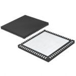 LTC2144IUP-12#PBF

The activity of extra discounts on wholesale prices is in full swing…
Please fill in your contact information and we will send you the latest wholesale price list.





