 ChipApex | Global Electronic Components Supplier

SEARCH
Search Product
Search Post
— IC芯片 | 连接器 | 传感器 | 被动器件 —
Search productSearch post
— IC芯片 | 连接器 | 传感器 | 被动器件 —
Consult the customer manager about the wholesale price.
consultation hotline:86-132-6715-2157
email:[email protected]
Contact the product manager for consultation. One-stop consultation is available.
Do you want a lower wholesale price? Please send us your inquiry and we will reply immediately.
LTC2324IUKG-12#PBF is listed in the Analog To Digital Converters (ADC) range at ChipApex. The manufacturer field lists Analog Devices Inc.. Its product description is IC ADC 12BIT SAR 52QFN. Review the specifications below when checking this part for your BOM.
The LTC2324IUKG-12#PBF is a quad, 12-bit + sign successive approximation register (SAR) analog-to-digital converter. It supports simultaneous sampling at 2Msps per channel with no latency. The device operates from a single 3.3V or 5V supply and features an 8Vp-p differential input range. Key electrical specifications include a typical Signal-to-Noise Ratio (SNR) of 78dB, ±0.5LSB Integral Nonlinearity (INL), and guaranteed 12-bit resolution without missing codes. It integrates a low-drift internal reference and offers CMOS or LVDS serial interface options.
Verify the ordering suffix #PBF indicates lead-free finish and tube packaging. Confirm the 'I' grade designation matches the required operating temperature range of –40°C to 85°C for the specific application environment. Ensure compatibility with the 52-lead QFN package dimensions during PCB layout.
Select this component when four channels of synchronized high-speed conversion are required. The I-grade variant is suitable for industrial environments requiring operation down to –40°C. Consider the power dissipation of approximately 40mW per channel at full sample rate and utilize nap or sleep modes if lower power consumption is necessary during inactive periods.
This part belongs to the LTC2324 family of quad SAR ADCs. The 'I' suffix denotes the industrial temperature range (-40°C to 85°C). The 'UKG' indicates the 52-lead 7mm x 8mm plastic QFN package. The '-12' specifies the 12-bit resolution variant within the series.
Public confirmed substitute part numbers: LTC2324CUKG-12#PBF (Commercial temp range), LTC2324HUKG-12#PBF (Extended temp range).
The maximum sampling frequency is 2 Msps per channel.
Yes, the internal reference buffers can be disabled by grounding the REFBUFEN pin, allowing external references in the range of 1.25V to 5V to drive the REFOUT pins.
In LVDS mode, the CMOS/LVDS pin is tied to OVDD. Data is output differentially on SDOA+/SDOA–, SDOB+/SDOB–, etc., and must be terminated with a 100Ω resistor at the receiver.
Explore related parts through Data Acquisition, Integrated Circuits (ICs), all product categories, ChipApex homepage.
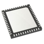 LTC2324IUKG-12#PBF

The activity of extra discounts on wholesale prices is in full swing…
Please fill in your contact information and we will send you the latest wholesale price list.




