 ChipApex | Global Electronic Components Supplier

SEARCH
Search Product
Search Post
— IC芯片 | 连接器 | 传感器 | 被动器件 —
Search productSearch post
— IC芯片 | 连接器 | 传感器 | 被动器件 —
Consult the customer manager about the wholesale price.
consultation hotline:86-132-6715-2157
email:[email protected]
Contact the product manager for consultation. One-stop consultation is available.
Do you want a lower wholesale price? Please send us your inquiry and we will reply immediately.
LTC2328HMS-18#TRPBF is listed in the Analog To Digital Converters (ADC) range at ChipApex. The manufacturer field lists Analog Devices Inc.. Its product description is IC ADC 18BIT SAR 16MSOP. Review the specifications below when checking this part for your BOM.
The LTC2328HMS-18#TRPBF is an 18-bit successive approximation register (SAR) analog-to-digital converter in a 16-lead MSOP package. It operates from a single 5V supply with a true bipolar input range of ±10.24V, achieving 95dB SNR and ±5LSB maximum INL. The device features a 1Msps sampling rate with no pipeline delay or cycle latency. It includes an onboard 2.048V temperature-compensated reference and a single-shot capable reference buffer. Power consumption is 50mW at full speed, scaling down to 300μW in sleep mode.
Verify the H-grade suffix indicates operation from -40°C to +125°C. Confirm the #TRPBF suffix denotes tape and reel packaging for automated assembly. Ensure OVDD supply voltage matches the host digital interface requirements between 1.71V and 5.25V.
Select this component for high-speed applications requiring wide dynamic range and true bipolar input handling without external level shifting. The internal reference simplifies design but may require overdriving with an external precision reference for lower drift specifications. Consider the 45pF input capacitance and acquisition time when designing the analog front-end driver circuit.
This part belongs to the LTC2328 family of SAR ADCs. The HMS-18 designation specifies the 18-bit resolution variant housed in a 16-lead MSOP package with extended industrial temperature range capabilities. It shares architectural similarities with the 16-bit LTC2328-16 but offers higher resolution and slightly different linearity specifications.
Public confirmed substitute part numbers are not available in the provided documentation. Verify pin compatibility and electrical parameters against existing designs if considering alternative manufacturers.
The device uses pseudo-differential inputs where IN+ accepts the signal and IN– serves as analog ground sense. An internal resistor divider network attenuates and level-shifts the ±2.5 • VREFBUF input swing to the ADC core's 0-VREFBUF range.
The device features a nap mode that reduces power dissipation proportionally with the sampling rate. Additionally, a sleep mode is provided to reduce power consumption to 300μW during inactive periods.
Yes, the internal reference buffer can be disabled by grounding the REFIN pin. This allows the REFBUF pin to be overdriven by an external reference voltage in the range of 2.5V to 5V.
Explore related parts through Data Acquisition, Integrated Circuits (ICs), all product categories, ChipApex homepage.
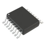 LTC2328HMS-18#TRPBF

The activity of extra discounts on wholesale prices is in full swing…
Please fill in your contact information and we will send you the latest wholesale price list.





