 ChipApex | Global Electronic Components Supplier
LTC2617IDE-1#TRPBF
Search Product
Search Post
— IC芯片 | 连接器 | 传感器 | 被动器件 —
Search productSearch post
— IC芯片 | 连接器 | 传感器 | 被动器件 —
Consult the customer manager about the wholesale price.
consultation hotline:86-132-6715-2157
email:[email protected]
Contact the product manager for consultation. One-stop consultation is available.
Do you want a lower wholesale price? Please send us your inquiry and we will reply immediately.
The LTC2617IDE-1#TRPBF is a dual 14-bit rail-to-rail voltage output digital-to-analog converter (DAC) in a 12-lead DFN package. It operates on a single supply of 2.7V to 5.5V and features an I²C compatible serial interface supporting standard (100kHz) and fast (400kHz) modes. The device includes built-in high-performance output buffers, double-buffered data latches, and an asynchronous DAC update pin (LDAC). This specific variant incorporates a power-on reset circuit that sets the voltage outputs to mid-scale upon initialization.
Verify the ordering suffix #TRPBF indicates tape and reel packaging. Confirm the 'IDE' designation corresponds to the industrial temperature range (-40°C to 85°C). Ensure the '-1' suffix matches the required mid-scale power-on reset behavior for the application design.
Select this part when a compact dual-channel solution is required. The 14-bit resolution offers a balance between precision and speed. Consider the -1 variant if mid-scale initialization is preferred over zero-scale. Verify I²C bus capacitance limits if operating in fast mode.
This component belongs to the LTC2607/LTC2617/LTC2627 family, which shares identical pinouts and interfaces but differs in resolution (16, 14, and 12 bits respectively). The LTC2617 provides 14-bit performance within the same tiny 3mm × 4mm DFN footprint as its 16-bit counterpart.
LTC2617IDE#TRPBF: Identical specifications except power-on reset defaults to zero scale instead of mid-scale.
The LTC2617-1 variant resets the voltage outputs to mid-scale until a valid write and update command is executed.
Addresses are selected by connecting the CA0, CA1, and CA2 pins to VCC, GND, or leaving them floating, providing 27 unique addresses plus a global address.
LDAC is an asynchronous DAC update pin. A falling edge updates the DAC register with the input register contents immediately, independent of the I²C clock.
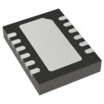 LTC2617IDE-1#TRPBF
The activity of extra discounts on wholesale prices is in full swing…
Please fill in your contact information and we will send you the latest wholesale price list.






