ChipApex | Global Electronic Components Supplier
LTC2621CDD#PBF
Search Product
Search Post
— IC芯片 | 连接器 | 传感器 | 被动器件 —
Search productSearch post
— IC芯片 | 连接器 | 传感器 | 被动器件 —
Consult the customer manager about the wholesale price.
consultation hotline:86-132-6715-2157
email:[email protected]
Contact the product manager for consultation. One-stop consultation is available.
Do you want a lower wholesale price? Please send us your inquiry and we will reply immediately.
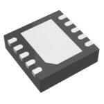
The LTC2621CDD#PBF is a single-channel, 12-bit rail-to-rail voltage output digital-to-analog converter (DAC) housed in a 10-lead 3mm × 3mm plastic DFN package. It operates on a single supply voltage ranging from 2.5V to 5.5V and features built-in high-performance output buffers capable of sourcing or sinking at least 15mA. The device utilizes a simple SPI/MICROWIRE compatible 3-wire serial interface with clock rates up to 50MHz. Key electrical specifications include a maximum differential nonlinearity (DNL) of ±0.5 LSB, integral nonlinearity (INL) of ±0.8 LSB, and a typical settling time of 7µs. Supply current is typically 300µA at 3V, reducing to 1µA maximum in power-down mode.
Verify the specific ordering suffix '#PBF' confirms lead-free finish and tube packaging as listed in the manufacturer's order information table. Confirm the 'C' grade designation corresponds to the commercial temperature range of 0°C to 70°C. Ensure the pinout matches the 10-lead DFN configuration with an exposed ground pad that must be soldered to the PCB for proper thermal and electrical performance.
Select the LTC2621CDD#PBF when a 12-bit resolution is sufficient for the application, offering higher speed and lower power compared to the 14-bit (LTC2611) or 16-bit (LTC2601) variants in the same family. Choose this part if the design requires a 3mm × 3mm footprint for board density optimization. Verify that the required operating temperature range aligns with the commercial grade (0°C to 70°C); for industrial ranges (-40°C to 85°C), select the IDD variant instead.
This component belongs to the LTC2601/LTC2611/LTC2621 family of single-supply DACs. It shares identical pinouts, interfaces, and physical dimensions with the 16-bit LTC2601 and 14-bit LTC2611, allowing for pin-compatible upgrades or downgrades based on resolution requirements. The CDD suffix indicates a commercial temperature grade, while the #PBF denotes a lead-free finish.
 LTC2621CDD#PBF
The activity of extra discounts on wholesale prices is in full swing…
Please fill in your contact information and we will send you the latest wholesale price list.