 ChipApex | Global Electronic Components Supplier
LTC2621IDD-1#PBF
Search Product
Search Post
— IC芯片 | 连接器 | 传感器 | 被动器件 —
Search productSearch post
— IC芯片 | 连接器 | 传感器 | 被动器件 —
Consult the customer manager about the wholesale price.
consultation hotline:86-132-6715-2157
email:[email protected]
Contact the product manager for consultation. One-stop consultation is available.
Do you want a lower wholesale price? Please send us your inquiry and we will reply immediately.
The LTC2621IDD-1#PBF is a single-channel, 12-bit rail-to-rail voltage output digital-to-analog converter (DAC) from Analog Devices. It operates on a 2.5V to 5.5V supply and features a built-in high-performance output buffer capable of sourcing or sinking at least 15mA. The device utilizes a simple SPI/Microwire compatible 3-wire serial interface with clock rates up to 50MHz. Key specifications include a settling time of 7µs, differential nonlinearity (DNL) of ±0.5 LSB, and integral nonlinearity (INL) of ±0.8 LSB. The -1 suffix indicates an integrated power-on reset circuit that sets the output to midscale upon initialization.
Verify the specific ordering suffix to confirm package type and lead finish. The '#PBF' suffix denotes a lead-free finish and tube packaging. Ensure the '-1' suffix is present if midscale power-on reset functionality is required for the application design.
Select this component when a single-channel, high-density 12-bit DAC is needed with rail-to-rail output swing. Compare against LTC2601 (16-bit) or LTC2611 (14-bit) if higher resolution is required. Verify that the 3-wire serial interface timing meets the system's microcontroller or DSP capabilities.
This part belongs to the LTC2601/LTC2611/LTC2621 family of 16/14/12-bit DACs. They share pin compatibility and similar electrical characteristics, differing primarily in resolution. The LTC2621 offers the lowest resolution but maintains the same small 10-lead DFN footprint and performance metrics as its higher-resolution counterparts.
LTC2621CDD-1#PBF (Commercial grade, 0°C to 70°C)
For the LTC2621-1 variant, the power-on reset circuit sets the voltage outputs to midscale until a valid write and update command are executed.
The LDAC pin allows for asynchronous DAC updates. A falling edge on LDAC immediately updates the DAC register with the contents of the input register, independent of the CS/LD signal state.
The serial interface supports clock rates up to 50MHz.
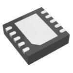 LTC2621IDD-1#PBF
The activity of extra discounts on wholesale prices is in full swing…
Please fill in your contact information and we will send you the latest wholesale price list.






