 ChipApex | Global Electronic Components Supplier
LTC2629IGN#PBF
Search Product
Search Post
— IC芯片 | 连接器 | 传感器 | 被动器件 —
Search productSearch post
— IC芯片 | 连接器 | 传感器 | 被动器件 —
Consult the customer manager about the wholesale price.
consultation hotline:86-132-6715-2157
email:[email protected]
Contact the product manager for consultation. One-stop consultation is available.
Do you want a lower wholesale price? Please send us your inquiry and we will reply immediately.
The LTC2629IGN#PBF is a quad 12-bit rail-to-rail voltage output digital-to-analog converter (DAC) in a 16-lead SSOP package. It operates on a single supply voltage ranging from 2.7V to 5.5V and features built-in high-performance output buffers. The device utilizes a 2-wire I²C compatible serial interface supporting standard (100kHz) and fast (400kHz) modes. Key electrical specifications include a settling time of 7µs, differential nonlinearity of ±0.5 LSB, and integral nonlinearity of ±1 LSB. It draws 1.25mA at 5V and supports individual channel power-down to 1µA.
Verify the suffix #PBF indicates lead-free finish and RoHS compliance. Confirm the IGN suffix corresponds to the industrial temperature range of -40°C to +85°C. Ensure the SSOP-16 package matches the target PCB footprint requirements.
Select this component when four independent 12-bit channels are required in a compact form factor. Choose the IGN variant over the CGN variant if operation below 0°C is necessary. Consider the LTC2629-1 variant if mid-scale power-on reset behavior is preferred over zero-scale.
This part belongs to the LTC2609/LTC2619/LTC2629 family of pin-compatible quad DACs. While maintaining identical pinouts and interfaces, the family differentiates by resolution: LTC2609 offers 16 bits, LTC2619 offers 14 bits, and the LTC2629 provides 12 bits. This allows for design flexibility without changing board layout.
The LTC2629CGN#PBF serves as a commercial grade replacement within the same package and specification profile, differing only in the operating temperature range (0°C to 70°C).
The LTC2629 incorporates a power-on reset circuit that sets the voltage outputs to zero-scale until a valid write and update command are executed.
There are 27 selectable slave addresses determined by the logic states (High, Low, or Floating) of the CA0, CA1, and CA2 pins.
The device guarantees a high rail-to-rail output drive of ±15mA minimum when VCC is 5V.
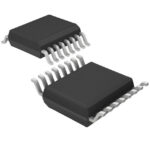 LTC2629IGN#PBF
The activity of extra discounts on wholesale prices is in full swing…
Please fill in your contact information and we will send you the latest wholesale price list.





