 ChipApex | Global Electronic Components Supplier
LTC2633AHTS8-HZ12#TRMPBF
Search Product
Search Post
— IC芯片 | 连接器 | 传感器 | 被动器件 —
Search productSearch post
— IC芯片 | 连接器 | 传感器 | 被动器件 —
Consult the customer manager about the wholesale price.
consultation hotline:86-132-6715-2157
email:[email protected]
Contact the product manager for consultation. One-stop consultation is available.
Do you want a lower wholesale price? Please send us your inquiry and we will reply immediately.
The LTC2633AHTS8-HZ12#TRMPBF is a dual 12-bit voltage-output digital-to-analog converter (DAC) from Analog Devices. It features an integrated precision reference with a full-scale output of 4.096V and operates on a single 4.5V to 5.5V supply. The device communicates via a 2-wire I²C-compatible serial interface supporting standard (100kHz) and fast (400kHz) modes. Key specifications include a maximum integral nonlinearity error of ±1.5 LSB, rail-to-rail output buffers, and guaranteed monotonicity over the –40°C to 125°C temperature range. Power-on reset defaults to zero-scale in internal reference mode.
Verify the #TRMPBF suffix indicates a 500-unit tape and reel packaging configuration. Confirm the H-grade designation matches the required –40°C to 125°C automotive temperature range for the specific application environment.
Select this part when a 4.096V full-scale output is required with high accuracy. Ensure the system supply voltage supports the 4.5V minimum operating requirement. Verify that the I²C address configuration via the CA0 pin aligns with other bus devices.
This component belongs to the LTC2633 family of dual DACs. The 'A' grade denotes improved linearity performance compared to standard grades. The 'H' suffix specifies the higher voltage range variant, while 'Z' configures the power-on reset state to zero-scale.
Public confirmed substitute part numbers are not available in the provided documentation. Consult Analog Devices for direct replacements or cross-reference options.
The 'Z' code indicates that upon power-up, the DAC outputs reset to zero-scale in internal reference mode.
The LTC2633-H series requires a supply voltage between 4.5V and 5.5V to achieve specified performance.
The CA0 pin sets the least significant bit of the I²C slave address. It can be tied to VCC, GND, or left floating to select one of three possible addresses.
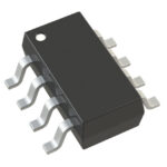 LTC2633AHTS8-HZ12#TRMPBF
The activity of extra discounts on wholesale prices is in full swing…
Please fill in your contact information and we will send you the latest wholesale price list.






