ChipApex | Global Electronic Components Supplier
LTC2633CTS8-HZ12#TRPBF
Search Product
Search Post
— IC芯片 | 连接器 | 传感器 | 被动器件 —
Search productSearch post
— IC芯片 | 连接器 | 传感器 | 被动器件 —
Consult the customer manager about the wholesale price.
consultation hotline:86-132-6715-2157
email:[email protected]
Contact the product manager for consultation. One-stop consultation is available.
Do you want a lower wholesale price? Please send us your inquiry and we will reply immediately.
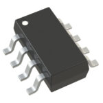
The LTC2633CTS8-HZ12#TRPBF is a dual 12-bit voltage-output digital-to-analog converter (DAC) from Analog Devices, housed in an 8-lead TSOT-23 package. It features an integrated precision reference with a full-scale output of 4.096V and operates on a single 4.5V to 5.5V supply. The device communicates via a 2-wire I²C-compatible serial interface supporting standard (100kHz) and fast (400kHz) modes. Key electrical specifications include a maximum integral nonlinearity (INL) error of ±1.5 LSB, a settling time of 4.7µs at 5V, and a typical supply current of 0.5mA. The part includes a power-on reset circuit configured to initialize outputs to zero-scale.
Verify the specific suffix #TRPBF indicates a 2,500-piece tape and reel packaging format as defined in the manufacturer's ordering information. Confirm that the C grade designation aligns with commercial temperature requirements if the application environment exceeds the standard 0°C to 70°C range, although the H-grade temperature performance is listed for the family.
Select this component when a dual-channel DAC with high accuracy (±1.5 LSB INL) and low power consumption is required in a compact TSOT-23 footprint. Ensure the system supply voltage remains within the 4.5V to 5.5V range specified for the H-grade internal reference configuration. Consider the zero-scale power-on reset feature if downstream circuits must remain inactive during initialization.
This part belongs to the LTC2633 family of dual DACs, which offers various combinations of resolution (8-, 10-, or 12-bit), full-scale voltage (2.5V or 4.096V), and power-on reset behaviors. The 'H' designation specifies the 4.096V full-scale output requiring a minimum 4.5V supply, while 'Z' denotes the zero-scale reset option. The 'A' electrical grade provides enhanced linearity compared to standard grades.
Direct replacements within the same family include LTC2633CTS8-HI12#TRPBF (mid-scale reset) or LTC2633CTS8-LZ12#TRPBF (2.5V full-scale). Verify pin compatibility and I²C address configurations when substituting parts with different power-on reset codes or reference voltages.
["What is the maximum integral nonlinearity (INL) error for the LTC2633CTS8-HZ12?","The maximum INL error is ±1.5 LSB for the 12-bit version."]
["How does the CA0 pin affect the device operation?","The CA0 pin serves as Chip Address Bit 0 for the I²C interface. Tying it to VCC, GND, or leaving it floating selects one of three available slave addresses."]
["What is the settling time for the DAC outputs?","The settling time is 4.7µs to ±1LSB (±0.024%) when operating at a 5V supply."]
 LTC2633CTS8-HZ12#TRPBF
The activity of extra discounts on wholesale prices is in full swing…
Please fill in your contact information and we will send you the latest wholesale price list.