 ChipApex | Global Electronic Components Supplier
LTC2633HTS8-LO12#TRMPBF
Search Product
Search Post
— IC芯片 | 连接器 | 传感器 | 被动器件 —
Search productSearch post
— IC芯片 | 连接器 | 传感器 | 被动器件 —
Consult the customer manager about the wholesale price.
consultation hotline:86-132-6715-2157
email:[email protected]
Contact the product manager for consultation. One-stop consultation is available.
Do you want a lower wholesale price? Please send us your inquiry and we will reply immediately.
The LTC2633HTS8-LO12#TRMPBF is a dual 12-bit voltage-output digital-to-analog converter (DAC) from Analog Devices, housed in an 8-lead TSOT-23 package. It features an integrated precision reference providing a full-scale output of 2.5V with a temperature coefficient of 10ppm/°C. The device operates on a single supply voltage ranging from 2.7V to 5.5V and communicates via a 2-wire I²C-compatible serial interface supporting standard (100kHz) and fast (400kHz) modes. Key electrical specifications include a maximum integral nonlinearity (INL) error of ±1.5 LSB, a settling time of 4.5µs at 3V for 12-bit accuracy, and a supply current of 0.4mA at 3V. The part is guaranteed monotonic over the –40°C to 125°C automotive temperature range.
Verify the specific ordering suffix #TRMPBF indicates a 500-unit tape and reel packaging configuration, distinct from the standard 2,500-unit reel. Confirm that the LO12 designation corresponds to the High Impedance power-on reset option for the 12-bit variant. Ensure compatibility with the required 2.7V to 5.5V supply range and I²C bus voltage levels before procurement.
Select this component when a dual-channel DAC with high initial output safety is required, as the LO suffix ensures outputs enter a high-impedance state upon power-up. Choose the H-grade version for automotive applications requiring operation between –40°C and 125°C. For lower cost requirements where mid-scale reset is acceptable, consider the LI12 variant. Verify that the 2.5V internal reference meets the system's full-scale voltage needs or if an external reference is necessary.
This part belongs to the LTC2633 family of dual DACs, which also includes variants with different resolutions (8-bit, 10-bit), reset behaviors (zero-scale, mid-scale), and reference voltages (4.096V). The HTS8 designation specifies the automotive temperature grade and the 8-lead TSOT-23 package type. The A suffix denotes the higher accuracy grade with ±1.5 LSB maximum INL compared to the standard ±2.5 LSB grade.
Direct pin-compatible replacements within the same package and function include other LTC2633 variants such as LTC2633HTS8-LI12#TRMPBF or LTC2633HTS8-HZ12#TRMPBF, provided the power-on reset behavior and supply voltage constraints align with the design requirements.
The 'O' code in the part number indicates that upon power-up, both DAC outputs are set to a high-impedance state while the internal reference remains active.
As an 'A' grade device, the LTC2633A-LO12 guarantees a maximum INL error of ±1.5 LSB across the specified temperature range.
Yes, although the internal reference is selected by default for the LO12 variant, the REF pin can be used to input an external reference voltage between 1V and VCC to set the full-scale output.
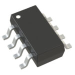 LTC2633HTS8-LO12#TRMPBF
The activity of extra discounts on wholesale prices is in full swing…
Please fill in your contact information and we will send you the latest wholesale price list.






