 ChipApex | Global Electronic Components Supplier
LTC2645IMS-L12#PBF
Search Product
Search Post
— IC芯片 | 连接器 | 传感器 | 被动器件 —
Search productSearch post
— IC芯片 | 连接器 | 传感器 | 被动器件 —
Consult the customer manager about the wholesale price.
consultation hotline:86-132-6715-2157
email:[email protected]
Contact the product manager for consultation. One-stop consultation is available.
Do you want a lower wholesale price? Please send us your inquiry and we will reply immediately.
The LTC2645IMS-L12#PBF is a quad 12-bit PWM-to-voltage output DAC from Analog Devices, housed in a 16-lead MSOP package. It integrates a high-accuracy, low-drift 10ppm/°C reference, providing a 2.5V full-scale output. The device measures PWM period and pulse width, updating outputs within 8µs typically. It operates on a single 2.7V to 5.5V supply with rail-to-rail buffered outputs capable of sourcing/sinking up to 5mA (3V) or 10mA (5V). Key specifications include ±2.5LSB max INL, ±1LSB max DNL, and guaranteed monotonicity over the industrial temperature range of –40°C to 85°C.
Verify the suffix #PBF indicates lead-free packaging and tube shipping format. Confirm the IMS designation corresponds to the industrial temperature grade (-40°C to 85°C) and MSOP package. Ensure compatibility with the required PWM input voltage levels (1.71V to 5.5V) and supply voltage range (2.7V to 5.5V) for the specific application design.
Select this part for applications requiring direct PWM input without external filtering or buffering. The 12-bit resolution and ±2.5LSB INL suit precision calibration tasks. Consider the idle mode options (zero-scale, full-scale, hold, or power-down) via the IDLSEL pin for system initialization requirements. External reference mode is available if a different full-scale voltage is needed.
This component belongs to the LTC2645 family, which includes 10-bit and 8-bit variants (LTC2645-L10, LTC2645-L8). The L12 suffix specifically denotes the 12-bit resolution version. Other family members share the same package, interface, and reference architecture but differ in linearity specifications and maximum PWM input frequencies.
Publicly confirmed substitute part numbers are not provided in the source documentation. Designers should evaluate other Analog Devices PWM DACs or general-purpose voltage output DACs based on interface compatibility and performance metrics if substitution is necessary.
The device measures the period and pulse width of the PWM input signals. It updates the corresponding voltage output after each rising edge of the PWM input, calculating the duty cycle to determine the digital code.
The IDLSEL pin selects the behavior of the DAC output when no PWM rising edge is received for more than 60ms. It can be configured for zero-scale, full-scale, hold previous state, or power-down with high impedance output.
Yes, by connecting the REFSEL pin to VCC, the device enters external reference mode. In this mode, the voltage supplied to the REF pin sets the full-scale output voltage, ranging from 1V to VCC.
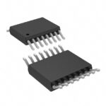 LTC2645IMS-L12#PBF
The activity of extra discounts on wholesale prices is in full swing…
Please fill in your contact information and we will send you the latest wholesale price list.





