 ChipApex | Global Electronic Components Supplier
SEARCH
Search Product
Search Post
— IC芯片 | 连接器 | 传感器 | 被动器件 —
Search productSearch post
— IC芯片 | 连接器 | 传感器 | 被动器件 —
Consult the customer manager about the wholesale price.
consultation hotline:86-132-6715-2157
email:[email protected]
Contact the product manager for consultation. One-stop consultation is available.
Do you want a lower wholesale price? Please send us your inquiry and we will reply immediately.
The LTC4300A-2CMS8#TRPBF is a hot swappable 2-wire bus buffer manufactured by Analog Devices Inc. It operates within a supply voltage range of 2.7V to 5.5V and supports data rates up to 400kHz. The device features bidirectional buffering for SDA and SCL lines, isolating backplane and card capacitances during live insertion. It includes rise-time accelerator circuitry that provides transient boosted pull-up currents, typically 12mA, to meet system requirements with weaker DC pull-ups. The component utilizes a dedicated VCC2 pin for level shifting between 3.3V and 5V systems and incorporates a 1V precharge function on all SDA and SCL lines to minimize bus disturbances.
Verify the specific ordering suffix TRPBF indicates tape and reel packaging when sourcing this component. Confirm the CMS8 designation corresponds to the commercial temperature range of 0°C to 70°C. Ensure compatibility with the 8-lead MSOP package dimensions for PCB layout. Cross-reference the manufacturer part number with official distributor catalogs to confirm current availability status.
Select the LTC4300A-2 variant specifically when level shifting between disparate supply voltages, such as 3.3V and 5V, is required. This model replaces the ENABLE pin found in the -1 variant with a VCC2 supply pin and an ACC input for controlling rise-time accelerators. Ensure the application does not require the low current disable feature provided by the ENABLE pin on the -1 version.
This component belongs to the LTC4300A series of hot swappable 2-wire bus buffers. It shares core functionality with the LTC4300A-1 but differs in control architecture. The -2 variant is designed for systems needing independent supply rails for the backplane and card sides, whereas the -1 uses a single supply and digital enable control.
LTC4300A-1CMS8#TRPBF: Replaces if level shifting is not needed and digital enable control is preferred.
It uses a dedicated VCC2 pin for the card side supply, allowing independent voltage levels ranging from 2.7V to 5.5V on both VCC and VCC2 without constraints on which is higher.
The ACC pin is a digital CMOS input that enables or disables the rise-time accelerator currents on all four SDA and SCL pins.
It precharges the SDA and SCL lines to 1V before connection and isolates the backplane and card capacitances until the start-up sequence is complete.
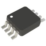 LTC4300A-2CMS8#TRPBF
The activity of extra discounts on wholesale prices is in full swing…
Please fill in your contact information and we will send you the latest wholesale price list.




