 ChipApex | Global Electronic Components Supplier

SEARCH
Search Product
Search Post
— IC芯片 | 连接器 | 传感器 | 被动器件 —
Search productSearch post
— IC芯片 | 连接器 | 传感器 | 被动器件 —
Consult the customer manager about the wholesale price.
consultation hotline:86-132-6715-2157
email:[email protected]
Contact the product manager for consultation. One-stop consultation is available.
Do you want a lower wholesale price? Please send us your inquiry and we will reply immediately.
LTC4301LCDD#PBF is listed in the Signal Buffers, Repeaters, Splitters range at ChipApex. The manufacturer field lists Analog Devices Inc.. Its product description is IC REDRIVER I2C HOTSWAP 2CH 8DFN. Review the specifications below when checking this part for your BOM.
The LTC4301LCDD#PBF is a hot swappable, supply-independent 2-wire bus buffer manufactured by Analog Devices Inc. It operates within a voltage range of 2.7V to 5.5V and supports I2C, I2C Fast Mode, and SMBus standards up to 600kHz. The device translates signals as low as 1V to standard logic rails while isolating input and output capacitances. It features 10kV Human Body Model ESD protection and includes a control circuitry that prevents bus corruption during live board insertion. The component is housed in an 8-lead DFN (3mm × 3mm) package and functions within a commercial temperature range of 0°C to 70°C.
Verify the specific suffix #PBF indicates lead-free packaging when sourcing this component. Confirm the LC designation corresponds to the commercial temperature range requirements for your target application environment. Ensure the DFN package footprint matches your PCB layout constraints before finalizing procurement orders.
Select the LTC4301LCDD#PBF when designing systems that require supply-independent level translation between varying bus voltages. This part is suitable for applications needing isolation between backplane and card capacitances to maintain signal integrity. Consider the 8-pin DFN package dimensions if space-constrained layouts are required for the interface circuitry.
This component belongs to the LTC4301 series of hot swappable bus buffers. It shares functional similarities with the LTC4300A but offers supply-independent operation. The DD suffix specifically denotes the 8-lead plastic DFN package format, distinguishing it from MSOP variants or tape-and-reel options within the same product family.
LTC4301CDD#PBF
The device provides bidirectional buffering that keeps backplane and card capacitances isolated. It regulates the output voltage slightly higher than the input voltage based on the pull-up resistance and VCC, ensuring proper logic levels across different supply rails.
For normal operation, the CS pin should be grounded. Driving CS above the 1.4V threshold isolates the input from the output and asserts the READY pin low, effectively disconnecting the backplane from the card until CS is pulled low again.
Yes, the device supports clock stretching, arbitration, and synchronization. The connection circuitry ensures that these protocols work correctly regardless of how devices on either side of the buffer are tied to the SDA and SCL lines.
Explore related parts through Interface, Integrated Circuits (ICs), all product categories, ChipApex homepage.
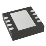 LTC4301LCDD#PBF

The activity of extra discounts on wholesale prices is in full swing…
Please fill in your contact information and we will send you the latest wholesale price list.




