 ChipApex | Global Electronic Components Supplier

SEARCH
Search Product
Search Post
— IC芯片 | 连接器 | 传感器 | 被动器件 —
Search productSearch post
— IC芯片 | 连接器 | 传感器 | 被动器件 —
Consult the customer manager about the wholesale price.
consultation hotline:86-132-6715-2157
email:[email protected]
Contact the product manager for consultation. One-stop consultation is available.
Do you want a lower wholesale price? Please send us your inquiry and we will reply immediately.
LTC4308IDD#PBF is listed in the Signal Buffers, Repeaters, Splitters range at ChipApex. The manufacturer field lists Analog Devices Inc.. Its product description is IC ACCELERATOR I2C HOTSWAP 8DFN. Review the specifications below when checking this part for your BOM.
The LTC4308IDD#PBF is a low voltage, level shifting hot swappable 2-wire bus buffer with stuck bus recovery. It supports I2C and SMBus protocols with a maximum operating frequency of 600 kHz. The supply voltage range is 2.3 V to 5.5 V, with a typical supply current of 7 mA. Propagation delay is 70 ns (high-to-low) and 10 ns (low-to-high). Input capacitance is 10 pF. The device operates from -40°C to +85°C and is housed in an 8-lead DFN package.
Verify the ordering suffix matches the required temperature grade and packaging format. The IDD suffix indicates the industrial temperature range (-40°C to +85°C). Confirm the PBF suffix denotes lead-free finish and RoHS compliance. Ensure the DFN package type aligns with the PCB footprint design requirements.
Select this component when hot swapping capabilities and automatic bus recovery are required. Verify that the system bus capacitance and pull-up resistor values allow the rise time accelerators to activate properly. Ensure the minimum supply voltage meets the 2.3 V requirement for reliable operation across the full temperature range.
This part belongs to the LTC4308 family of hot swappable bus buffers. It is functionally similar to the LTC4301L but includes additional features such as automatic stuck bus recovery and rise time accelerators. The IDD variant specifically covers the industrial temperature range and uses the DFN package.
When replacing an LTC4301L, account for the active-high ENABLE pin versus the active-low CS pin. Verify that the lower minimum supply voltage of 2.3 V is compatible with the system power rails. Ensure the application can tolerate the automatic clock generation during stuck bus recovery events.
If SDAOUT or SCLOUT remains low for 30ms, the device disconnects the input-output connection and generates up to 16 clock pulses on SCLOUT to attempt to free the bus.
READY is an open-drain output that indicates whether the input and output busses are connected. It goes low when ENABLE is low or during a stuck bus disconnection event.
Yes, it provides bidirectional level shifting between bus supplies as low as 0.9V and up to 5.5V, utilizing negative offset voltages to maintain compatibility.
Explore related parts through Interface, Integrated Circuits (ICs), all product categories, ChipApex homepage.
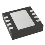 LTC4308IDD#PBF

The activity of extra discounts on wholesale prices is in full swing…
Please fill in your contact information and we will send you the latest wholesale price list.





