ChipApex | Global Electronic Components Supplier

SEARCH
Search Product
Search Post
— IC芯片 | 连接器 | 传感器 | 被动器件 —
Search productSearch post
— IC芯片 | 连接器 | 传感器 | 被动器件 —
Consult the customer manager about the wholesale price.
consultation hotline:86-132-6715-2157
email:[email protected]
Contact the product manager for consultation. One-stop consultation is available.
Do you want a lower wholesale price? Please send us your inquiry and we will reply immediately.
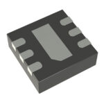
LTC6255CDC#TRMPBF is listed in the Instrumentation, Op Amps, Buffer Amps range at ChipApex. The manufacturer field lists Analog Devices Inc.. Its product description is IC OPAMP GP 1 CIRCUIT 6DFN. Review the specifications below when checking this part for your BOM.
The LTC6255CDC#TRMPBF is a single operational amplifier from Analog Devices, featuring rail-to-rail input and output capabilities. It operates on supply voltages ranging from 1.8V to 5.25V with a typical quiescent current of 65µA per amplifier. The device offers a gain-bandwidth product of 6.5MHz and a slew rate of 1.8V/µs. Key electrical specifications include a maximum input offset voltage of 350µV, a maximum input bias current of 50nA, and common mode rejection and power supply rejection ratios of 100dB. It is housed in a 6-lead (2mm × 2mm × 0.8mm) plastic DFN package.
Verify the specific suffix #TRMPBF indicates tape and reel packaging with mini-reel quantities. Confirm the CDC designation corresponds to the commercial temperature range of 0°C to 70°C. Ensure the lead-free finish matches project requirements. Cross-reference the manufacturer part number with official Analog Devices documentation to validate authenticity and revision status before procurement.
Select this component for applications requiring low power consumption alongside high bandwidth. The rail-to-rail I/O capability makes it suitable for single-supply systems operating at low voltages like 1.8V. Consider the shutdown feature if power management is critical. Verify that the 65µA quiescent current meets system budget constraints compared to higher-performance but more power-hungry alternatives.
This part belongs to the LTC6255/LTC6256/LTC6257 family of micropower, low distortion op amps. While the LTC6255 is a single channel, the family includes dual and quad variants. The CDC suffix specifically denotes the commercial grade version in a 6-lead DFN package, distinct from industrial or automotive grades which may offer wider temperature ranges.
Consult official Analog Devices documentation for verified pin-compatible substitutes within the same family. Ensure any replacement maintains the 6.5MHz gain-bandwidth product and 65µA supply current characteristics. Verify that the alternative package matches the 6-lead DFN footprint and thermal requirements.
Yes, the device features C-Load technology, allowing it to drive capacitive loads up to 100nF while maintaining unity gain stability.
The inputs are rail-to-rail, extending from V– – 0.1V to V+ + 0.1V, allowing for ground sensing and operation beyond the supply rails.
Driving the SHDN pin below 0.6V above the negative rail shuts down the amplifier, reducing supply current to a maximum of 7µA and placing the output in a high-impedance state.
Explore related parts through Amplifiers, Linear, Integrated Circuits (ICs), all product categories.
 LTC6255CDC#TRMPBF

The activity of extra discounts on wholesale prices is in full swing…
Please fill in your contact information and we will send you the latest wholesale price list.