 ChipApex | Global Electronic Components Supplier
SEARCH
Search Product
Search Post
— IC芯片 | 连接器 | 传感器 | 被动器件 —
Search productSearch post
— IC芯片 | 连接器 | 传感器 | 被动器件 —
Consult the customer manager about the wholesale price.
consultation hotline:86-132-6715-2157
email:[email protected]
Contact the product manager for consultation. One-stop consultation is available.
Do you want a lower wholesale price? Please send us your inquiry and we will reply immediately.
The LTC6360CDD#PBF is a single-supply, very low noise amplifier designed for driving SAR ADCs. It features a total output noise density of 2.3nV/√Hz and achieves a settling time of 150ns to 16-bit levels for a 4V step. The device operates on a single 5V supply but swings output to true zero via an internal charge pump generating approximately -0.6V. Key electrical parameters include a maximum input offset voltage of 900µV (DD8 package), gain-bandwidth product of 1GHz, and shutdown current under 350µA. It is housed in an 8-lead 3mm × 3mm DFN package with an exposed pad.
Verify the specific temperature grade 'C' corresponds to the 0°C to 70°C operating range required for your design environment. Confirm that the 8-lead DFN package footprint matches your PCB layout constraints. Ensure the application circuit accommodates the exposed pad connection to ground as specified in the datasheet pin configuration.
Select this component when a single-supply solution is required that must drive signals down to 0V without external negative rails. Compare the 900µV maximum offset voltage against system accuracy requirements. Consider the 1GHz gain-bandwidth product for high-frequency signal integrity needs. Evaluate the thermal performance within the 3mm × 3mm DFN package for your specific power dissipation limits.
This part belongs to the LTC6360 family of ultra-low noise amplifiers. The 'CDD' suffix indicates the 8-lead plastic DFN package variant with a commercial temperature range of 0°C to 70°C. Other variants in the series include the IDD (industrial) and HDD (extended) temperature grades, offering wider operational ranges while maintaining identical electrical specifications.
Direct substitutes within the same package and specification profile include the LTC6360IDD#PBF for industrial temperature ranges (-40°C to 85°C) and the LTC6360HDD#PBF for extended ranges (-40°C to 125°C). Verify that any replacement maintains the 3mm × 3mm DFN form factor and pinout compatibility.
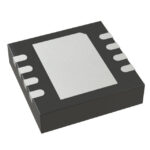 LTC6360CDD#PBF
The activity of extra discounts on wholesale prices is in full swing…
Please fill in your contact information and we will send you the latest wholesale price list.





