 ChipApex | Global Electronic Components Supplier

SEARCH
Search Product
Search Post
— IC芯片 | 连接器 | 传感器 | 被动器件 —
Search productSearch post
— IC芯片 | 连接器 | 传感器 | 被动器件 —
Consult the customer manager about the wholesale price.
consultation hotline:86-132-6715-2157
email:[email protected]
Contact the product manager for consultation. One-stop consultation is available.
Do you want a lower wholesale price? Please send us your inquiry and we will reply immediately.
LTC6952IUKG#PBF is listed in the Clock Generators, PLLs, Frequency Synthesizers range at ChipApex. The manufacturer field lists Analog Devices Inc.. Its product description is IC CLOCK GENERATOR 52QFN. Review the specifications below when checking this part for your BOM.
The LTC6952IUKG#PBF is a high-performance, ultralow jitter clock generation and distribution IC supporting JESD204B/C standards. It features an integrated Phase Locked Loop (PLL) core with a reference divider, phase-frequency detector, ultralow noise charge pump, and integer feedback divider. The device provides eleven independent outputs, configurable as up to five JESD204B/C Subclass 1 device clock/SYSREF pairs plus one general-purpose output, or eleven general-purpose clocks. Each output includes individually programmable frequency dividers and drivers. Key electrical parameters include a maximum output frequency of 4.5 GHz, a reference input frequency up to 500 MHz, and additive output jitter of less than 6 fs RMS (12kHz to 20MHz integration bandwidth at 4.5 GHz).
Verify the specific ordering suffix against manufacturer documentation to confirm package type and temperature range. The #PBF suffix indicates lead-free finish and RoHS compliance. Confirm availability status directly with authorized distributors, as supply conditions may vary. Ensure the procurement channel provides valid traceability documents consistent with Analog Devices Inc. specifications.
Select this component when designing systems requiring precise phase alignment across multiple devices using JESD204B/C Subclass 1. The LTC6952IUKG#PBF is suitable for applications needing up to eleven synchronized outputs with programmable delays. Consider the 52-lead QFN package constraints and thermal requirements, as the exposed pad must be soldered to the PCB ground plane. Verify that the system's reference input frequency does not exceed 500 MHz and that the VCO input supports the required frequency range up to 4.5 GHz.
The LTC6952 belongs to Analog Devices' family of high-performance clock generators designed for demanding communication and data acquisition applications. It is distinct from lower-output-count synthesizers by providing eleven fully independent outputs with dedicated delay controls. The IUKG package designation identifies the 52-lead (7mm × 8mm) Plastic QFN form factor used in this specific part number.
Publicly confirmed substitute part numbers are not available in the provided source material. Evaluate alternative clock synthesizers based on output count, jitter specifications, and JESD204B/C support compatibility if direct replacement is required.
The maximum differential output frequency is 4.5 GHz when configured in Clock Mode (MODEx = 0).
Up to five outputs can be configured as JESD204B/C Subclass 1 device clock/SYSREF pairs, with the remaining outputs available as general-purpose clocks or additional SYSREF signals.
The additive output jitter is less than 6 fs RMS with an integration bandwidth of 12 kHz to 20 MHz at an output frequency of 4.5 GHz.
Explore related parts through Clock/Timing, Integrated Circuits (ICs), all product categories, ChipApex homepage.
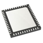 LTC6952IUKG#PBF

The activity of extra discounts on wholesale prices is in full swing…
Please fill in your contact information and we will send you the latest wholesale price list.







