 ChipApex | Global Electronic Components Supplier
SEARCH
Search Product
Search Post
— IC芯片 | 连接器 | 传感器 | 被动器件 —
Search productSearch post
— IC芯片 | 连接器 | 传感器 | 被动器件 —
Consult the customer manager about the wholesale price.
consultation hotline:86-132-6715-2157
email:[email protected]
Contact the product manager for consultation. One-stop consultation is available.
Do you want a lower wholesale price? Please send us your inquiry and we will reply immediately.
The LV5609V-TLM-E is a vertical clock driver for CCD sensors manufactured by onsemi. It operates within a supply voltage range of 2 V to 5.5 V and supports an input-to-output ratio of 7:5. The device features CMOS input and output logic levels, with one internal circuit configured for non-differential signal handling. It is housed in a 20-LSSOP package (4.40 mm width) designed for surface-mount assembly. The component functions reliably across an operating temperature range of -20°C to +80°C.
Verify the current lifecycle status of the LV5609V-TLM-E before design finalization, as distributor records indicate potential end-of-life or discontinuation. Confirm availability through authorized channels and check for any pending production change notices that may affect long-term supply stability.
Select this component when a dedicated vertical clock driver for CCDs is required with a 2 V to 5.5 V supply range. Ensure the design accommodates the 20-LSSOP footprint and the specified -20°C to +80°C operating temperature limits. Verify that the 7:5 ratio meets the specific timing requirements of the target CCD sensor.
This part belongs to the broader category of application-specific clock and timing integrated circuits. It serves a specialized function in imaging systems, distinct from general-purpose clock generators or distribution buffers. The device integrates specific logic required for CCD vertical scanning operations.
Publicly confirmed substitute part numbers are not available in the provided documentation. Consult manufacturer resources for obsolescence management or equivalent functional alternatives if this component is discontinued.
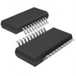 LV5609V-TLM-E
The activity of extra discounts on wholesale prices is in full swing…
Please fill in your contact information and we will send you the latest wholesale price list.






