 ChipApex | Global Electronic Components Supplier
LX256EV-5F484I
Search Product
Search Post
— IC芯片 | 连接器 | 传感器 | 被动器件 —
Search productSearch post
— IC芯片 | 连接器 | 传感器 | 被动器件 —
Consult the customer manager about the wholesale price.
consultation hotline:86-132-6715-2157
email:[email protected]
Contact the product manager for consultation. One-stop consultation is available.
Do you want a lower wholesale price? Please send us your inquiry and we will reply immediately.
The LX256EV-5F484I is a high-performance analog and digital crosspoint switch IC manufactured by Lattice Semiconductor. It features a 256 x 256 I/O switch matrix configuration designed for complex signal routing applications. The device supports data rates up to 38 Gb/s, enabling high-bandwidth connectivity. It operates with a nominal supply voltage of 2.5 V, with a specified range between 2.3 V and 2.7 V. The component utilizes an FPBGA-484 surface-mount package suitable for automated assembly. Input and output interfaces support multiple standards including Bus LVDS, LVCMOS, LVPECL, and LVTTL. The internal architecture integrates SERDES capabilities with a propagation delay of 5 ns. It functions within a commercial temperature range from 0°C to +90°C.
Verify the specific suffix 'I' indicates industrial temperature rating compliance if required for your environment. Confirm the 'EV' variant designation against current Lattice product announcements as legacy part numbers may have superseded versions. Check for end-of-life notifications or obsolescence warnings prior to final design approval. Ensure the FPBGA-484 footprint matches your PCB layout constraints. Validate that the 2.5V power domain aligns with your system's power management strategy.
Select this component when a large-scale crosspoint matrix is required rather than discrete switching solutions. Consider the 38 Gb/s data rate capability for future-proofing high-bandwidth links. Evaluate the multi-voltage I/O support to simplify interface design across different logic families. Assess the thermal performance within the 0°C to +90°C range against your enclosure conditions. Compare the pin count and package size against available board space.
This device belongs to Lattice's portfolio of analog and digital crosspoint switches, distinct from their FPGA lines such as ECP3 or CertusPro-NX. While FPGAs offer programmable logic, this IC specializes in dedicated signal routing and switching. It complements Lattice's broader communication and networking IC category. The LX256 series provides scalable switching density for professional audio/video and telecom markets.
Publicly confirmed substitute part numbers are not available in the provided documentation. Consult Lattice Semiconductor directly for current equivalent products or next-generation replacements. Verify if newer series within the LX family offer improved specifications or availability.
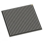 LX256EV-5F484I
The activity of extra discounts on wholesale prices is in full swing…
Please fill in your contact information and we will send you the latest wholesale price list.





