 ChipApex | Global Electronic Components Supplier
LX256V-35F484C
Search Product
Search Post
— IC芯片 | 连接器 | 传感器 | 被动器件 —
Search productSearch post
— IC芯片 | 连接器 | 传感器 | 被动器件 —
Consult the customer manager about the wholesale price.
consultation hotline:86-132-6715-2157
email:[email protected]
Contact the product manager for consultation. One-stop consultation is available.
Do you want a lower wholesale price? Please send us your inquiry and we will reply immediately.
The LX256V-35F484C is a digital crosspoint switch IC from the ispGDX2 family, manufactured by Lattice Semiconductor. It features a 256 x 256 configuration with a data rate of 38 Gb/s. The device operates at 1.8 V with a voltage range of 1.65 V to 1.95 V. Input and output types include Bus LVDS, LVCMOS, LVDS, LVPECL, and LVTTL. It supports SERDES interfaces and has a propagation delay of 3.5 ns. The component is housed in an FPBGA-484 package and operates between 0°C and +90°C.
Verify current availability status as this component may be discontinued or subject to end-of-life notifications. Confirm exact ordering suffixes match required speed grades and package variants. Check for authorized distributor channels to ensure authenticity. Review datasheet revisions for any functional updates or pinout changes before integration into new designs.
Select this part when a high-port-count digital crosspoint solution is required for signal distribution. Ensure system requirements align with the 38 Gb/s data rate capability and 1.8 V power domain. Verify that the FPBGA-484 package fits the board layout constraints. Consider thermal management within the specified operating temperature range during design.
This component belongs to the ispGDX2 family of programmable logic devices from Lattice Semiconductor. These devices are specialized for high-performance I/O and crosspoint switching applications. The family targets communication and networking markets requiring flexible signal routing capabilities.
Check for direct substitutes within the ispGDX2 family such as LX256V-35FN484C if available. Verify compatibility with existing system architectures before transitioning to alternative parts.
The device supports a maximum data rate of 38 Gb/s.
It supports Bus LVDS, LVCMOS, LVDS, LVPECL, and LVTTL input and output types.
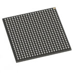 LX256V-35F484C
The activity of extra discounts on wholesale prices is in full swing…
Please fill in your contact information and we will send you the latest wholesale price list.





