 ChipApex | Global Electronic Components Supplier

SEARCH
Search Product
Search Post
— IC芯片 | 连接器 | 传感器 | 被动器件 —
Search productSearch post
— IC芯片 | 连接器 | 传感器 | 被动器件 —
Consult the customer manager about the wholesale price.
consultation hotline:86-132-6715-2157
email:[email protected]
Contact the product manager for consultation. One-stop consultation is available.
Do you want a lower wholesale price? Please send us your inquiry and we will reply immediately.
The Microsemi LX6431AIDM is a high-performance Field Programmable Gate Array (FPGA) belonging to the SmartFusion2 mixed-signal system-on-chip family. It integrates an Arm Cortex-M3 processor with Flash-based non-volatile memory and analog peripherals on a single die. Key specifications include 64,000 logic blocks for digital implementation, up to 5.76 Mbits of embedded Flash memory, and support for various serial and parallel communication interfaces. The device operates within a temperature range of -40°C to +100°C and is available in an 816-ball FineLine BGA package.
Verify the specific suffix codes on the component marking against the official datasheet to confirm package type, temperature grade, and lead-free status. Ensure compatibility with your design toolchain version, as programming utilities may require updates for newer silicon revisions. Confirm supply chain authenticity through authorized distributors to avoid counterfeit parts, especially for legacy or specialized FPGA families.
Select this component when a design requires tight integration of real-time control and flexible logic without separate microcontroller and FPGA chips. Consider the total I/O count and memory requirements against the 64k logic block limit. Evaluate the analog peripheral needs to determine if the integrated ADC/DAC resolution suffices or if external precision components are necessary. Check power budget constraints as the integrated processor and Flash impact active current draw.
This part belongs to the Microsemi SmartFusion2 family, which bridges the gap between pure ASICs and discrete FPGA/MCU solutions. It is designed for applications needing security, low power, and rapid time-to-market. The family supports both standard and industrial temperature ranges, offering flexibility for harsh environment deployments while maintaining pin-to-pin compatibility within certain package variants.
Direct replacements are limited due to the unique mixed-signal architecture. Consider Microsemi IGLOO2 or PolarFire SoC series for similar integration levels but different performance profiles. Cross-vendor alternatives like Xilinx Zynq-7000 or Intel Cyclone V SoC require significant schematic and firmware redesigns due to differing processor cores and peripheral sets.
Yes, the device supports standard JTAG interface for boundary scan testing and in-system programming/debugging via the dedicated debug port.
The embedded Arm Cortex-M3 processor typically operates at frequencies up to 100 MHz, depending on the specific voltage and temperature conditions defined in the datasheet.
Yes, the embedded Flash memory is electrically erasable and reprogrammable, allowing for field updates and configuration changes without UV exposure.
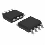 LX6431AIDM

The activity of extra discounts on wholesale prices is in full swing…
Please fill in your contact information and we will send you the latest wholesale price list.





