 ChipApex | Global Electronic Components Supplier

SEARCH
Search Product
Search Post
— IC芯片 | 连接器 | 传感器 | 被动器件 —
Search productSearch post
— IC芯片 | 连接器 | 传感器 | 被动器件 —
Consult the customer manager about the wholesale price.
consultation hotline:86-132-6715-2157
email:[email protected]
Contact the product manager for consultation. One-stop consultation is available.
Do you want a lower wholesale price? Please send us your inquiry and we will reply immediately.
LXB0104T14-13 is listed in the Translators, Level Shifters range at ChipApex. The manufacturer field lists Diodes Incorporated. Its product description is IC. Review the specifications below when checking this part for your BOM.
The LXB0104 is a 4-bit bi-directional level translator designed for push-pull applications. It incorporates a buffered architecture with edge rate accelerators to achieve data rates up to 110Mbps during 3.3V to 5.0V translation. The device supports universal low-voltage translation between A port (1.2V to 3.6V) and B port (1.65V to 5.5V). It features an active-high OE pin for high-impedance control, IOFF circuitry for partial power-down protection, and ESD protection exceeding JESD 22 standards.
Verify the specific package type required for the design, as the LXB0104 is available in U-QFN1720-12, TSSOP-14, and V-QFN3535-14 configurations. Confirm that the ordering suffix matches the desired packing quantity and reel size. Ensure the driver strength meets the minimum ±2mA requirement for proper operation. Check for automotive-compliant variants if operating under stricter environmental conditions.
Select this component when interfacing logic families with varying supply voltages, specifically where A port operates at 1.2V to 3.6V and B port at 1.65V to 5.5V. Ensure VCCA does not exceed VCCB during operation. Consider the IOFF feature if the system requires safe handling during partial power-down states. Verify that the application utilizes push-pull CMOS logic outputs, as open-drain configurations are not supported by this specific architecture.
The LXB0104 belongs to Diodes Incorporated's LXB series of bi-directional level translators. It is distinct from the LSF0204QT14-13, which targets different speed or voltage requirements. An automotive-compliant version, designated LXB0104Q, is available under a separate datasheet for applications requiring extended qualification standards beyond standard industrial specifications.
LXB0104Q
The device driving the data I/Os must have a drive strength of at least ±2mA for proper operation.
The OE pin should be tied to GND through a pulldown resistor before VCCA becomes stable to ensure a high-impedance OFF-state. It should never be left floating.
The IOFF circuitry disables the output to prevent damaging backflow current through the device when it is powered down, ensuring safe partial power-down mode operation.
Explore related parts through Logic, Integrated Circuits (ICs), all product categories, ChipApex homepage.
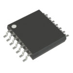 LXB0104T14-13

The activity of extra discounts on wholesale prices is in full swing…
Please fill in your contact information and we will send you the latest wholesale price list.






