 ChipApex | Global Electronic Components Supplier

SEARCH
Search Product
Search Post
— IC芯片 | 连接器 | 传感器 | 被动器件 —
Search productSearch post
— IC芯片 | 连接器 | 传感器 | 被动器件 —
Consult the customer manager about the wholesale price.
consultation hotline:86-132-6715-2157
email:[email protected]
Contact the product manager for consultation. One-stop consultation is available.
Do you want a lower wholesale price? Please send us your inquiry and we will reply immediately.
M74HC597B1R is listed in the Shift Registers range at ChipApex. The manufacturer field lists STMicroelectronics. Its product description is IC LATCH/SHIFT REG 8BIT 16-DIP. Review the specifications below when checking this part for your BOM.
The M74HC597B1R is an 8-bit parallel-in, serial-out (PISO) shift register with a storage latch, manufactured using high-speed silicon gate C2MOS technology. It operates within a supply voltage range of 2V to 6V and supports a maximum clock frequency of 50 MHz at 6V. The device features asynchronous reset and direct load inputs, positive edge-triggered clocks for both the storage and shift registers, and balanced propagation delays. It provides symmetrical output impedance with a minimum drive current of 4mA and includes protection circuits against static discharge.
Verify the specific package type required, as the M74HC597 family is available in DIP, SOP, and TSSOP configurations. Confirm that the B1R suffix corresponds to the Tube packaging format specified in the ordering codes. Ensure compatibility with the target system's voltage levels and temperature requirements before finalizing procurement.
Select this component when an 8-bit PISO configuration with a dedicated storage latch is required. It is suitable for designs needing high-speed operation up to 50 MHz and wide voltage flexibility between 2V and 6V. Consider the pin count and package dimensions relative to the PCB layout constraints.
This part belongs to the STMicroelectronics M74HC597 series of high-speed CMOS logic devices. It is functionally compatible with the standard 74HC597 architecture, ensuring interoperability with other components from various manufacturers that adhere to the same logical specifications and pinout definitions.
Direct substitutes include the SN74HC597 from Texas Instruments or the CD74HC597 from Texas Instruments, which share identical logical functions and pinouts. Verify package compatibility and electrical characteristics such as propagation delay and drive current when cross-referencing alternative sources.
SCK is the Shift Clock input that advances data through the shift register stages on the rising edge. RCK is the Storage Clock input that transfers the data from the shift register to the storage latch outputs on the rising edge.
When SLOAD is active low, it loads the parallel data present on inputs A through H directly into the storage register, bypassing the shift register sequence.
Explore related parts through Logic, Integrated Circuits (ICs), all product categories, ChipApex homepage.
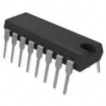 M74HC597B1R

The activity of extra discounts on wholesale prices is in full swing…
Please fill in your contact information and we will send you the latest wholesale price list.






