ChipApex | Global Electronic Components Supplier
SEARCH
Search Product
Search Post
— IC芯片 | 连接器 | 传感器 | 被动器件 —
Search productSearch post
— IC芯片 | 连接器 | 传感器 | 被动器件 —
Consult the customer manager about the wholesale price.
consultation hotline:86-132-6715-2157
email:[email protected]
Contact the product manager for consultation. One-stop consultation is available.
Do you want a lower wholesale price? Please send us your inquiry and we will reply immediately.
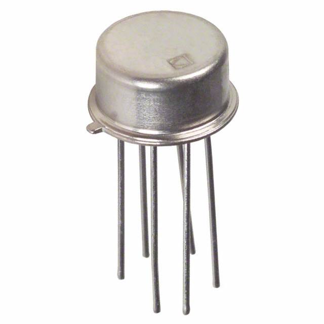
The MAT03EH is a low noise, matched dual PNP transistor manufactured by Analog Devices Inc. It features a TO-78 metal can package and operates within an extended industrial temperature range of -40°C to +85°C. Key electrical specifications at 25°C include a maximum offset voltage of 100 µV, a minimum current gain of 100, and a typical gain bandwidth of 190 MHz. The device exhibits a maximum noise voltage density of 1 nV/√Hz at 1 kHz and a bulk resistance typically ranging from 0.3 Ω to 0.75 Ω. Absolute maximum ratings specify a collector-base voltage of 36 V and total power dissipation of 500 mW in free air.
Verify the specific suffix EH against the ordering guide to confirm the 100 µV offset voltage limit and TO-78 packaging. Ensure electrostatic discharge precautions are implemented during handling due to device sensitivity. Confirm that the application environment remains within the specified -40°C to +85°C operating temperature range to guarantee performance parameters.
Select the MAT03EH when a maximum offset voltage of 100 µV is required rather than the 200 µV limit of the MAT03FH variant. Consider the TO-78 package constraints for thermal management, as power dissipation must be derated above 70°C ambient temperature. Evaluate the need for internal ESD protection if external clamping is not present in the circuit design.
The MAT03 series consists of low noise, matched dual PNP transistors designed for high-frequency and precision analog applications. The MAT03EH represents the version with tighter offset voltage specifications compared to other variants in the family. These devices are fabricated using monolithic technology to ensure consistent matching between the two integrated transistors.
Publicly confirmed substitute part numbers are not available in the provided documentation. Designers should verify pin compatibility and electrical parameter overlaps with alternative matched transistor arrays before substitution.
The maximum offset voltage (VOS) for the MAT03EH is 100 µV at 25°C.
Internal protection diodes across the base-emitter junction clamp any reverse potential to prevent breakdown conditions that could degrade gain and matching performance.
The typical gain bandwidth is 190 MHz.
 MAT03EH
The activity of extra discounts on wholesale prices is in full swing…
Please fill in your contact information and we will send you the latest wholesale price list.