 ChipApex | Global Electronic Components Supplier
SEARCH
Search Product
Search Post
— IC芯片 | 连接器 | 传感器 | 被动器件 —
Search productSearch post
— IC芯片 | 连接器 | 传感器 | 被动器件 —
Consult the customer manager about the wholesale price.
consultation hotline:86-132-6715-2157
email:[email protected]
Contact the product manager for consultation. One-stop consultation is available.
Do you want a lower wholesale price? Please send us your inquiry and we will reply immediately.
The MAT14ARZ is a quad monolithic NPN transistor from Analog Devices Inc., housed in a 14-lead SOIC package. It provides excellent parametric matching for precision amplifier and nonlinear circuit applications. Key electrical characteristics include a minimum current gain of 300, maximum offset voltage of 400 µV, and maximum noise voltage density of 3 nV/√Hz at 100 Hz with IC = 1 mA. The device features a bulk resistance (rBE) of 0.6 Ω maximum and operates within an ambient temperature range of -40°C to +85°C.
Verify the ordering suffix against the manufacturer's official documentation to confirm specific packaging options such as tube or reel configurations. Ensure the component meets RoHS compliance requirements if mandated by your design specifications. Cross-reference the part number with the latest datasheet revision to confirm operating temperature ranges and electrical limits before finalizing procurement.
Select the MAT14ARZ when precise matching between multiple transistors is critical for circuit accuracy. Consider its low noise density and high current gain for applications requiring signal integrity over wide collector current ranges. Verify that the 14-lead SOIC package dimensions fit the available PCB space and thermal management constraints of the target system design.
The MAT14 belongs to Analog Devices' portfolio of matched transistor arrays designed for high-precision analog signal processing. Unlike discrete transistors, this monolithic integration guarantees superior tracking of parameters like offset voltage and current gain across temperature variations, making it suitable for demanding instrumentation and nonlinear processing tasks.
Consult the manufacturer's ordering guide for alternative packaging options including MAT14ARZ-R7 and MAT14ARZ-RL. No direct cross-manufacturer substitutes are documented in the provided source material; verify compatibility through detailed parameter comparison if considering alternatives.
Each transistor includes protection diodes across the base-emitter junction to prevent degradation of beta and matching characteristics caused by reverse bias or base-emitter current.
The maximum noise voltage density is 3 nV/√Hz at 100 Hz with a collector current of 1 mA.
The typical offset voltage is 100 µV, with a maximum limit of 400 µV under standard test conditions.
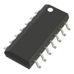 MAT14ARZ
The activity of extra discounts on wholesale prices is in full swing…
Please fill in your contact information and we will send you the latest wholesale price list.





