 ChipApex | Global Electronic Components Supplier

SEARCH
Search Product
Search Post
— IC芯片 | 连接器 | 传感器 | 被动器件 —
Search productSearch post
— IC芯片 | 连接器 | 传感器 | 被动器件 —
Consult the customer manager about the wholesale price.
consultation hotline:86-132-6715-2157
email:[email protected]
Contact the product manager for consultation. One-stop consultation is available.
Do you want a lower wholesale price? Please send us your inquiry and we will reply immediately.
MAX11158EUB+ is listed in the Analog To Digital Converters (ADC) range at ChipApex. The manufacturer field lists Analog Devices Inc./Maxim Integrated. Its product description is IC ADC 18BIT SAR 10UMAX. Review the specifications below when checking this part for your BOM.
The MAX11158EUB+ is an 18-bit, 500ksps successive approximation register (SAR) analog-to-digital converter. It features a true bipolar input range of ±5V while operating from a single 5V analog supply and a separate 2.3V to 5V digital supply. The device integrates a low-drift internal reference with a buffer, achieving 93.7dB SNR and -100.0dB THD at 10kHz. It guarantees 18-bit no-missing codes with typical INL of ±2.7 LSB and DNL of ±0.5 LSB. Communication occurs via an SPI-compatible serial interface supporting daisy-chaining and busy indicators.
Verify component authenticity through authorized Analog Devices distributors or certified partners. Request original manufacturer datasheets and RoHS compliance documentation upon inquiry. Confirm package integrity and pin alignment against the 10-pin µMAX specification before integration into production workflows.
Select this component when bipolar ±5V input signals must be digitized directly using a single 5V supply. Ensure the driving source impedance remains below 1kΩ for optimal settling within the 500ns acquisition window. Verify that the host controller supports the required SPI timing parameters for the chosen interface mode.
This part belongs to the MAX11158 family of 18-bit SAR ADCs. It is distinguished by its ±5V input capability and integrated reference, unlike the MAX11168 which offers 16-bit resolution, or the MAX11150 which accepts 0V to 5V inputs. It shares the compact 10-pin µMAX package form factor common to this series.
Direct functional substitutes include the MAX11168 for 16-bit applications or the MAX11150 for unipolar requirements. Cross-referencing pinouts and thermal characteristics is essential when replacing these variants in existing designs.
The device includes input clamping circuits that activate if AIN+ exceeds VDD + 300mV or drops below -(VDD + 300mV). These clamps remain high-impedance within normal operation but limit voltage during faults to protect the internal circuitry.
The logic level of the SDI pin during the rising edge of the CNVST signal determines the mode. If SDI is high, CS mode is selected; if SDI is low, daisy-chain mode is enabled.
An external buffer is recommended if the source impedance causes significant settling errors within the 500ns acquisition period. Direct driving is suitable for source impedances less than 1kΩ.
Explore related parts through Data Acquisition, Integrated Circuits (ICs), all product categories, ChipApex homepage.
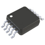 MAX11158EUB+

The activity of extra discounts on wholesale prices is in full swing…
Please fill in your contact information and we will send you the latest wholesale price list.





