 ChipApex | Global Electronic Components Supplier

SEARCH
Search Product
Search Post
— IC芯片 | 连接器 | 传感器 | 被动器件 —
Search productSearch post
— IC芯片 | 连接器 | 传感器 | 被动器件 —
Consult the customer manager about the wholesale price.
consultation hotline:86-132-6715-2157
email:[email protected]
Contact the product manager for consultation. One-stop consultation is available.
Do you want a lower wholesale price? Please send us your inquiry and we will reply immediately.
MAX1179CCUI+ is listed in the Analog To Digital Converters (ADC) range at ChipApex. The manufacturer field lists Analog Devices Inc./Maxim Integrated. Its product description is IC ADC 16BIT SAR 28TSSOP. Review the specifications below when checking this part for your BOM.
The MAX1179CCUI+ is a 16-bit successive-approximation analog-to-digital converter (ADC) manufactured by Analog Devices Inc./Maxim Integrated. It features a single +4.75V to +5.25V analog supply and interfaces with digital logic ranging from +2.7V to +5.25V. The device supports a sampling rate of 135ksps and accepts a bipolar analog input voltage range of ±5V. It includes an internal clock, automatic power-down capabilities, and a 16-bit wide parallel interface. The component is housed in a 28-pin TSSOP package and operates within a commercial temperature range of 0°C to +70°C.
Verify the specific suffix 'C' indicates the commercial temperature range (0°C to +70°C) rather than the extended range ('E'). Confirm the part status as discontinued or obsolete through official manufacturer channels before finalizing procurement plans. Ensure compatibility with existing board layouts regarding the 28-pin TSSOP footprint.
Select this component when a 16-bit resolution and ±5V bipolar input range are required. Compare against MAX1187 (0 to +10V unipolar) and MAX1189 (±10V bipolar) if different input ranges suit the application better. Consider the 135ksps sampling rate and low-power shutdown mode for battery-operated systems requiring high accuracy.
This part belongs to the MAX1179/MAX1187/MAX1189 family of 16-bit, low-power SAR ADCs. These devices share identical architectures and pinouts but differ in analog input voltage ranges and temperature specifications. The MAX1179 specifically targets applications requiring a ±5V input range within the commercial temperature grade.
MAX1179ACUI+
Holding the R/C pin low during the second falling edge of CS places the device in standby mode, keeping the reference active. Setting R/C high during that same edge initiates shutdown mode, powering down the reference and buffer to minimize current.
When waking up from shutdown mode, the internal reference requires a minimum of 12ms to settle before starting a new conversion, assuming standard bypass capacitor values of 10µF on REF and 0.1µF on REFADJ.
In shutdown mode, the input current is minimal. Upon transitioning to acquisition mode, the input current steps to its operating value. Driving circuits must be capable of settling within the acquisition time to maintain accuracy.
Explore related parts through Data Acquisition, Integrated Circuits (ICs), all product categories, ChipApex homepage.
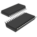 MAX1179CCUI+

The activity of extra discounts on wholesale prices is in full swing…
Please fill in your contact information and we will send you the latest wholesale price list.




