 ChipApex | Global Electronic Components Supplier

SEARCH
Search Product
Search Post
— IC芯片 | 连接器 | 传感器 | 被动器件 —
Search productSearch post
— IC芯片 | 连接器 | 传感器 | 被动器件 —
Consult the customer manager about the wholesale price.
consultation hotline:86-132-6715-2157
email:[email protected]
Contact the product manager for consultation. One-stop consultation is available.
Do you want a lower wholesale price? Please send us your inquiry and we will reply immediately.
MAX1240BESA+T is listed in the Analog To Digital Converters (ADC) range at ChipApex. The manufacturer field lists Analog Devices Inc./Maxim Integrated. Its product description is IC ADC 12BIT SAR 8SOIC. Review the specifications below when checking this part for your BOM.
The MAX1240BESA+T is a single-channel, 12-bit successive-approximation analog-to-digital converter (ADC) manufactured by Analog Devices Inc. under the Maxim Integrated brand. It operates on a single +2.7V to +3.6V supply and features an internal 2.5V reference voltage. The device supports a maximum sampling rate of 73 kS/s with a throughput clock frequency up to 2.1MHz. It utilizes a 3-wire serial interface compatible with SPI, QSPI, and MICROWIRE protocols. Key electrical specifications include a signal-to-noise ratio of 70 dB, differential nonlinearity of ±1 LSB, and integral nonlinearity of ±0.5 LSB. The component is housed in an 8-pin SO package and functions within a temperature range of -40°C to +85°C.
Verify the specific suffix 'V+' indicates automotive qualification and lead-free compliance when sourcing this part number. Confirm the package type matches the required PCB footprint. Ensure the operating environment falls within the specified industrial temperature range. Cross-reference the datasheet revision to confirm pinout consistency. Validate supplier authenticity to prevent counterfeit components.
Select the MAX1240BESA+T when a single-ended input and internal reference are required. Compare against the MAX1241 if a wider supply voltage range up to 5.25V is necessary. Consider the power consumption at the target sampling rate. Evaluate the serial interface compatibility with the host microcontroller. Assess the need for automotive qualification versus commercial grade options.
This component belongs to the MAX1240/MAX1241 family of low-power, 12-bit serial ADCs. The MAX1240 variant distinguishes itself by including an internal 2.5V reference, whereas the MAX1241 requires an external reference source. Both share identical architectural features and performance characteristics. The family targets applications demanding small form factors and minimal power consumption.
The TSM1285BESA+ is documented as an alternate source for the MAX1285 and serves as a higher-speed upgrade path relative to the MAX1240 series. Verify pin compatibility and interface timing requirements before substitution. Check if the replacement meets the specific voltage and accuracy constraints of the design.
The internal 2.5V reference is enabled by pulling the SHDN pin high. Leaving the SHDN pin open disables the internal reference, allowing the use of an external reference voltage at the REF pin.
The minimum acquisition time is 1.5µs. This duration ensures the internal hold capacitor charges sufficiently based on the source impedance and internal resistance.
The DOUT pin transitions from high impedance to logic low during conversion and then goes high to signal the end of conversion (EOC). Data bits are shifted out on subsequent falling edges of the SCLK.
Explore related parts through Data Acquisition, Integrated Circuits (ICs), all product categories, ChipApex homepage.
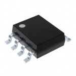 MAX1240BESA+T

The activity of extra discounts on wholesale prices is in full swing…
Please fill in your contact information and we will send you the latest wholesale price list.




