 ChipApex | Global Electronic Components Supplier

SEARCH
Search Product
Search Post
— IC芯片 | 连接器 | 传感器 | 被动器件 —
Search productSearch post
— IC芯片 | 连接器 | 传感器 | 被动器件 —
Consult the customer manager about the wholesale price.
consultation hotline:86-132-6715-2157
email:[email protected]
Contact the product manager for consultation. One-stop consultation is available.
Do you want a lower wholesale price? Please send us your inquiry and we will reply immediately.
MAX1246ACEE+ is listed in the Analog To Digital Converters (ADC) range at ChipApex. The manufacturer field lists Analog Devices Inc./Maxim Integrated. Its product description is IC ADC 12BIT SAR 16QSOP. Review the specifications below when checking this part for your BOM.
The MAX1246ACEE+ is a 12-bit successive-approximation analog-to-digital converter (ADC) featuring a 4-channel multiplexer and high-bandwidth track/hold circuit. It operates from a single +2.7V to +3.6V supply with an internal 2.5V reference. The device supports software-configurable unipolar or bipolar inputs and utilizes a 4-wire serial interface compatible with SPI, QSPI, and MICROWIRE protocols. Key electrical specifications include a sampling rate of 133ksps, a signal-to-noise ratio of 70dB, and integral nonlinearity of ±0.5 LSB. It is housed in a 16-pin QSOP package and functions within a temperature range of 0°C to +70°C.
Verify the component authenticity by checking the manufacturer markings against official datasheet specifications. Confirm the specific suffix 'ACEE+' corresponds to the commercial temperature range and lead-free packaging requirements. Ensure the ordering information matches the exact pin configuration and package dimensions required for the target PCB layout.
Select this component when a low-power, 12-bit resolution ADC is required for battery-operated systems. The internal reference simplifies design compared to the MAX1247 variant, which requires an external reference. Ensure the system clock frequency supports the desired sampling rate and that the serial interface timing aligns with the host microcontroller's SPI or Microwire settings.
This part belongs to the MAX1246/MAX1247 family of low-power, serial 12-bit ADCs. It shares architectural similarities with the MAX186 and MAX146 series but offers a compact 16-pin QSOP footprint comparable to an 8-pin SO package. The device is designed to replace older parallel ADCs in space-constrained applications requiring moderate speed and precision.
Public confirmed substitute part numbers are not available in the provided documentation. Designers should verify compatibility with existing board layouts if considering alternative packages or pinouts from other manufacturers.
In differential mode, the device samples the difference between two channels selected from pairs CH0/CH1 and CH2/CH3. The return side must remain stable within ±0.5LSB relative to AGND during conversion.
The SHDN pin controls the shutdown state. Pulling it low shuts down the device, while pulling it high enables the internal reference-buffer amplifier. Floating the pin places the buffer in external compensation mode.
Yes, the device can use either an internal clock or an external serial-interface clock. In external clock mode, the SCLK frequency determines the conversion speed, up to 2MHz.
Explore related parts through Data Acquisition, Integrated Circuits (ICs), all product categories, ChipApex homepage.
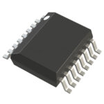 MAX1246ACEE+

The activity of extra discounts on wholesale prices is in full swing…
Please fill in your contact information and we will send you the latest wholesale price list.





