 ChipApex | Global Electronic Components Supplier

SEARCH
Search Product
Search Post
— IC芯片 | 连接器 | 传感器 | 被动器件 —
Search productSearch post
— IC芯片 | 连接器 | 传感器 | 被动器件 —
Consult the customer manager about the wholesale price.
consultation hotline:86-132-6715-2157
email:[email protected]
Contact the product manager for consultation. One-stop consultation is available.
Do you want a lower wholesale price? Please send us your inquiry and we will reply immediately.
MAX1246BCEE+ is listed in the Analog To Digital Converters (ADC) range at ChipApex. The manufacturer field lists Analog Devices Inc./Maxim Integrated. Its product description is IC ADC 12BIT SAR 16QSOP. Review the specifications below when checking this part for your BOM.
The MAX1246BCEE+ is a low-power, serial-output, 12-bit analog-to-digital converter (ADC) housed in a 16-pin QSOP package. It integrates a 4-channel multiplexer, high-bandwidth track/hold circuitry, and an internal 2.5V reference. Operating from a single +2.7V to +3.6V supply, it achieves sampling rates up to 133ksps with a typical supply current of 1.2mA. The device features software-configurable unipolar or bipolar inputs and supports SPI/QSPI/MICROWIRE interfaces. Key accuracy specifications include ±1 LSB INL and DNL, a signal-to-noise ratio of 70dB, and a small-signal bandwidth of 2.25MHz.
Verify the component against official Analog Devices documentation to confirm the specific B-grade accuracy class and QSOP-16 packaging. Ensure the design accommodates the required +2.7V to +3.6V supply range and thermal dissipation limits for the plastic package. Cross-reference the ordering suffix to guarantee compatibility with the intended temperature range and performance specifications.
Select this component when a compact 12-bit ADC with integrated multiplexing and reference is required for space-constrained designs. It is suitable for applications needing low power consumption during idle periods and software-configurable input ranges. Consider the MAX1247 variant if operation above 3.6V or an external reference is necessary.
This part belongs to the MAX1246/MAX1247 family of serial ADCs. The MAX1246 variant distinguishes itself by including an internal reference, whereas the MAX1247 requires an external one. Both share identical architectures but differ in supply voltage capabilities and reference configurations.
The MAX1247ACEE+ serves as a functional alternative within the same family, offering similar performance but requiring an external reference and supporting higher supply voltages up to 5.25V.
In differential mode, the device samples the difference between two channels selected from pairs CH0/CH1 and CH2/CH3. This configuration is pseudo-differential, requiring the return side to remain stable within ±0.5LSB relative to AGND during conversion.
Pulling the SHDN pin high places the reference-buffer amplifier into internal compensation mode. Leaving the pin floating configures the amplifier for external compensation mode.
No, the datasheet recommends using internal clock mode if the serial clock frequency is less than 100kHz to prevent excessive droop on the sample-and-hold capacitors.
Explore related parts through Data Acquisition, Integrated Circuits (ICs), all product categories, ChipApex homepage.
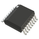 MAX1246BCEE+

The activity of extra discounts on wholesale prices is in full swing…
Please fill in your contact information and we will send you the latest wholesale price list.




