 ChipApex | Global Electronic Components Supplier

SEARCH
Search Product
Search Post
— IC芯片 | 连接器 | 传感器 | 被动器件 —
Search productSearch post
— IC芯片 | 连接器 | 传感器 | 被动器件 —
Consult the customer manager about the wholesale price.
consultation hotline:86-132-6715-2157
email:[email protected]
Contact the product manager for consultation. One-stop consultation is available.
Do you want a lower wholesale price? Please send us your inquiry and we will reply immediately.
MAX1294BCEI is listed in the Analog To Digital Converters (ADC) range at ChipApex. The manufacturer field lists Analog Devices Inc./Maxim Integrated. Its product description is IC ADC 12BIT SAR 28QSOP. Review the specifications below when checking this part for your BOM.
The MAX1294BCEI is a low-power, 12-bit analog-to-digital converter (ADC) featuring a successive-approximation architecture. It operates from a single +5V supply and includes an on-chip clock, a +2.5V internal reference, and a high-speed 12-bit parallel interface. The device supports a maximum sampling rate of 420ksps with power consumption of 10mW at full speed. It offers software-configurable analog inputs for unipolar/bipolar and single-ended/pseudo-differential operation, providing six input channels in single-ended mode. The component is housed in a 28-pin QSOP package and functions within a temperature range of 0°C to +70°C.
Verify the specific ordering suffix against official manufacturer documentation to confirm the exact temperature grade and package variant. Ensure that any additional characters following the base model number correspond precisely to the intended specifications before finalizing procurement orders.
Select this component when a 12-bit resolution and up to 420ksps sampling rate are required within a +5V system. Consider the 28-pin QSOP footprint and the availability of an internal reference when designing compact data-acquisition circuits.
This part belongs to the MAX1294/MAX1296 family of precision ADCs. It shares architectural similarities with the MAX1291/MAX1293 series but differs in operating voltage (+5V vs +3V) and channel count. The 'B' designation indicates a specific linearity class within the product lineup.
For pin-compatible +3V versions, consult the MAX1295 or MAX1297 datasheets. Verify electrical characteristics and supply voltage requirements before substituting other devices in existing designs.
Internal protection diodes clamp the analog inputs to VDD and GND, allowing signals to swing within (GND - 300mV) to (VDD + 300mV) without damage.
The INT pin goes low to indicate that the conversion is complete and output data is ready. It returns high upon the first read cycle or if a new control byte is written.
Yes, the device supports both internal and external clock modes. External clock frequencies between 100kHz and 7.6MHz are recommended for proper operation.
Explore related parts through Data Acquisition, Integrated Circuits (ICs), all product categories, ChipApex homepage.
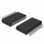 MAX1294BCEI

The activity of extra discounts on wholesale prices is in full swing…
Please fill in your contact information and we will send you the latest wholesale price list.




