 ChipApex | Global Electronic Components Supplier

SEARCH
Search Product
Search Post
— IC芯片 | 连接器 | 传感器 | 被动器件 —
Search productSearch post
— IC芯片 | 连接器 | 传感器 | 被动器件 —
Consult the customer manager about the wholesale price.
consultation hotline:86-132-6715-2157
email:[email protected]
Contact the product manager for consultation. One-stop consultation is available.
Do you want a lower wholesale price? Please send us your inquiry and we will reply immediately.
MAX14821ETG+ is listed in the Drivers, Receivers, Transceivers range at ChipApex. The manufacturer field lists Analog Devices Inc./Maxim Integrated. Its product description is IC TRANSCEIVER 1/1 24TQFN. Review the specifications below when checking this part for your BOM.
The MAX14821ETG+ is an IO-Link device transceiver designed for 24V binary sensors and actuators. It supports IO-Link Versions 1.0 and 1.1.2 with COM1, COM2, and COM3 data rates up to 230.4 kbps. The device operates on a VCC supply of 9V to 36V and includes integrated 5V and 3.3V linear regulators. It features independently configurable C/Q and DO drivers supporting push-pull, PNP, or NPN configurations with 100mA drive capability. The component is housed in a 4mm x 4mm, 24-pin TQFN package and operates within a temperature range of -40°C to +85°C.
Verify the specific suffix ETG+ against official manufacturer documentation to confirm the exact package type and RoHS compliance status. Ensure that the ordering information matches the required pin configuration and thermal characteristics for your design implementation.
Select this component when designing IO-Link devices requiring integrated power regulation and robust fault protection. Consider the TQFN package dimensions and thermal resistance values if space constraints or heat dissipation are critical factors in the system layout.
This part belongs to the Maxim Integrated MAX14821 series of IO-Link transceivers. It serves as a physical layer interface between microcontrollers running data-link protocols and 24V field devices, consolidating signal conditioning and power management functions into a single compact solution.
Consult official Analog Devices documentation for verified substitute part numbers. Do not assume functional equivalence with other models without reviewing specific electrical parameter differences.
The device detects short circuits lasting longer than 140µs and enters an autoretry mode. It periodically checks for the fault condition every 26ms and attempts to correct the output during 240µs intervals.
The VL pin defines the logic levels for all logic inputs and outputs. It accepts a voltage range of 2.3V to 5.5V and determines the threshold voltages for SPI and control signals.
Yes, the internal 5V LDO can be disabled by connecting the LDOIN pin directly to the V5 pin. In this configuration, an external voltage between 4.75V and 5.25V must be applied to V5.
Explore related parts through Interface, Integrated Circuits (ICs), all product categories, ChipApex homepage.
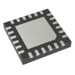 MAX14821ETG+

The activity of extra discounts on wholesale prices is in full swing…
Please fill in your contact information and we will send you the latest wholesale price list.





