 ChipApex | Global Electronic Components Supplier

SEARCH
Search Product
Search Post
— IC芯片 | 连接器 | 传感器 | 被动器件 —
Search productSearch post
— IC芯片 | 连接器 | 传感器 | 被动器件 —
Consult the customer manager about the wholesale price.
consultation hotline:86-132-6715-2157
email:[email protected]
Contact the product manager for consultation. One-stop consultation is available.
Do you want a lower wholesale price? Please send us your inquiry and we will reply immediately.
MAX1491CNI+ is listed in the ADCs/DACs - Special Purpose range at ChipApex. The manufacturer field lists Analog Devices Inc./Maxim Integrated. Its product description is IC DRVR 7 SEG 3 1/2 DIGIT 28DIP. Review the specifications below when checking this part for your BOM.
The MAX1491CNI+ is a low-power, single-chip analog-to-digital converter (ADC) with an integrated liquid crystal display (LCD) driver. It provides 3.5-digit resolution (±1999 count) using a sigma-delta architecture. The device operates from a single 2.7V to 5.25V supply and includes an internal 2.048V reference, high-accuracy oscillator, and charge pump for negative supply generation. It features selectable input ranges of ±2V or ±200mV, on-chip buffers for high-impedance sources, and >100dB rejection of 50Hz/60Hz line noise. The part is housed in a 28-pin DIP package and operates over the 0°C to +70°C temperature range.
Verify the suffix 'CNI+' indicates the commercial temperature range (0°C to +70°C) and 28-pin DIP package configuration. Confirm RoHS compliance status through official manufacturer documentation prior to integration. Ensure the ordering code matches the specific pinout and resolution requirements for the target design.
Select this component for applications requiring direct LCD interfacing without external microcontrollers. The ±200mV range offers higher resolution for small signals, while the ±2V range suits broader measurements. Verify that the source impedance remains within limits for the internal buffers and that the supply voltage stays between 2.7V and 5.25V.
This part belongs to the MAX1491/MAX1493/MAX1495 family of single-chip ADCs with LCD drivers. While the MAX1493 and MAX1495 provide 4.5-digit resolution in TQFP packages, the MAX1491 variant specifically delivers 3.5-digit resolution. The 'C' denotes the commercial temperature range, and 'NI' specifies the 28-pin DIP package style.
Direct replacements within the same family include the MAX1491CAI (SSOP package). For higher resolution needs, the MAX1493CCJ or MAX1495CCJ offer 4.5-digit performance in a 32-pin TQFP package. Package pinouts differ significantly between DIP, SSOP, and TQFP variants; verify mechanical compatibility before substitution.
An internal charge pump generates a negative supply voltage (VNEG) at the VNEG pin. This allows the analog input buffers to accept bipolar signals ranging from -2.2V to +2.2V relative to ground.
The device operates at a fixed conversion rate of 5Hz, corresponding to the SINC4 digital filter's settling time of four output data periods.
Yes. By connecting the INTREF pin to GND, the device switches to external reference mode. In this mode, REF+ and REF- must be bypassed to GND with capacitors >= 0.1µF.
Explore related parts through Data Acquisition, Integrated Circuits (ICs), all product categories, ChipApex homepage.
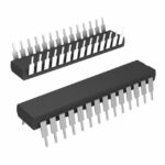 MAX1491CNI+

The activity of extra discounts on wholesale prices is in full swing…
Please fill in your contact information and we will send you the latest wholesale price list.





