 ChipApex | Global Electronic Components Supplier
MAX15024AATB/V+T
Search Product
Search Post
— IC芯片 | 连接器 | 传感器 | 被动器件 —
Search productSearch post
— IC芯片 | 连接器 | 传感器 | 被动器件 —
Consult the customer manager about the wholesale price.
consultation hotline:86-132-6715-2157
email:[email protected]
Contact the product manager for consultation. One-stop consultation is available.
Do you want a lower wholesale price? Please send us your inquiry and we will reply immediately.
The MAX15024AATB/V+T is a single low-side gate driver from Analog Devices, designed for high-speed MOSFET switching. It features a peak output current of 8A sink and 4A source capabilities with propagation delays as low as 16ns. The device operates within an input voltage range of 4.5V to 28V and supports both inverting and non-inverting logic configurations. Qualified under AEC-Q100 standards, it functions reliably across temperatures from -40°C to +125°C. Packaged in a thermally enhanced TDFN-10 (3mm x 3mm) footprint, it offers efficient power dissipation suitable for compact automotive and industrial applications.
Verify the specific suffix 'V+' indicates lead-free compliance and tape-and-reel packaging configuration. Confirm that the TDFN-10 thermal pad soldering requirements are met during assembly. Ensure the operating supply voltage remains within the 4.5V to 28V range to prevent device damage. Check for any regional distribution restrictions or limited availability status before finalizing procurement plans.
Select this component when high-speed switching with minimal propagation delay is critical for system efficiency. The 8A sink current makes it suitable for driving larger MOSFETs compared to lower-current alternatives. Consider the AEC-Q100 qualification if the application requires automotive reliability standards. The single-channel configuration is ideal for simple half-bridge setups rather than complex multi-phase arrangements.
This part belongs to the MAX15024 family of single and dual gate drivers optimized for high-current applications. It complements other Maxim Integrated solutions by providing a compact, high-performance option for low-side switching. The series emphasizes speed and robustness, targeting demanding environments where traditional drivers may lack sufficient current capacity or switching speed.
Direct substitutes include the MAX15024AATB+T and MAX15024AATB/V+T variants within the same product line. Cross-reference pinout compatibility and electrical specifications carefully when considering alternative manufacturers' parts to ensure functional equivalence in high-speed switching scenarios.
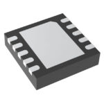 MAX15024AATB/V+T
The activity of extra discounts on wholesale prices is in full swing…
Please fill in your contact information and we will send you the latest wholesale price list.






