 ChipApex | Global Electronic Components Supplier

SEARCH
Search Product
Search Post
— IC芯片 | 连接器 | 传感器 | 被动器件 —
Search productSearch post
— IC芯片 | 连接器 | 传感器 | 被动器件 —
Consult the customer manager about the wholesale price.
consultation hotline:86-132-6715-2157
email:[email protected]
Contact the product manager for consultation. One-stop consultation is available.
Do you want a lower wholesale price? Please send us your inquiry and we will reply immediately.
MAX199AENI+ is listed in the ADCs/DACs - Special Purpose range at ChipApex. The manufacturer field lists Analog Devices Inc./Maxim Integrated. Its product description is IC DAS 12BIT 100K 28DIP. Review the specifications below when checking this part for your BOM.
The MAX199AENI+ is a multi-range, 12-bit data-acquisition system (DAS) from Analog Devices Inc./Maxim Integrated. It operates on a single +5V supply and converts analog signals up to ±4V at its inputs. The device features eight independently software-programmable analog input channels with selectable ranges: ±VREF, ±VREF/2, 0V to VREF, or 0V to VREF/2. This configuration increases the effective dynamic range to 14 bits. Key electrical specifications include a 100ksps throughput rate, 6µs conversion time, and a 5MHz bandwidth track/hold circuit. The unit includes fault protection for inputs up to ±16.5V and supports both internal and external clock and reference sources.
Verify the specific suffix 'ENI+' against the manufacturer's current ordering information to confirm package type (Narrow Plastic DIP), temperature range (0°C to +70°C), and lead-free status. Ensure compatibility with existing board layouts for the 28-pin DIP footprint. Cross-reference the revision date of the datasheet to confirm any updates to timing characteristics or absolute maximum ratings prior to final procurement.
Select this component when a single +5V supply is required for an 8-channel acquisition system with flexible input ranging. The MAX199A variant offers tighter accuracy specifications compared to the MAX199B. Consider the internal 4.096V reference capability if external reference buffering is undesirable. Ensure the microprocessor interface timing matches the TTL/CMOS compatible three-state data I/O requirements.
The MAX199 series serves as a multi-range DAS solution, distinct from the MAX197 which offers different input ranges (±10V, ±5V). It differs from the MAX196/MAX198 by utilizing an 8+4 parallel bus interface rather than a 12-bit bus interface. The MAX199A denotes the higher accuracy grade within the family, suitable for precision applications requiring stricter linearity and offset error limits.
For alternative input ranges such as ±10V or ±5V, consult the MAX197 datasheet. For devices requiring a 12-bit bus interface, refer to the MAX196 or MAX198 documentation. No direct pin-compatible substitutes are listed in the provided source material; verify functional equivalence carefully if considering other manufacturers' parts.
The internal 2.50V reference is buffered with a gain of 1.6384 to provide 4.096V at the REF pin. The REFADJ pin allows adjustment of this voltage by ±1.5% using an external resistor network connected between REFADJ, AGND, and VDD.
The HBEN pin controls the output data format. When HBEN is low, the lower eight bits (LSBs) are available on the data bus. When HBEN is high, the upper four MSBs are multiplexed onto the data bus, allowing full 12-bit data retrieval in two steps.
The input channels are fault-protected to ±16.5V. This protection remains active even in power-down modes. A fault condition on any channel will not affect the conversion result of the selected channel.
Explore related parts through Data Acquisition, Integrated Circuits (ICs), all product categories, ChipApex homepage.
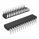 MAX199AENI+

The activity of extra discounts on wholesale prices is in full swing…
Please fill in your contact information and we will send you the latest wholesale price list.





