 ChipApex | Global Electronic Components Supplier

SEARCH
Search Product
Search Post
— IC芯片 | 连接器 | 传感器 | 被动器件 —
Search productSearch post
— IC芯片 | 连接器 | 传感器 | 被动器件 —
Consult the customer manager about the wholesale price.
consultation hotline:86-132-6715-2157
email:[email protected]
Contact the product manager for consultation. One-stop consultation is available.
Do you want a lower wholesale price? Please send us your inquiry and we will reply immediately.
The MAX22506EAUA+ is a half-duplex RS-485/RS-422 transceiver manufactured by Analog Devices Inc./Maxim Integrated. It supports data rates up to 50Mbps and operates on a supply voltage range of 3V to 5.5V. The device features integrated ESD protection rated at ±15kV (Human Body Model) and ±7kV IEC 61000-4-2 air-gap discharge. It includes fail-safe receiver functionality that ensures a logic-high output when inputs are shorted or open for longer than 10μs. The component is housed in an 8-pin μMAX package and operates within a temperature range of -40°C to +125°C.
Verify the specific ordering suffix against official documentation to confirm package type and RoHS compliance status. Confirm availability through authorized distributors as stock levels fluctuate. Ensure the procurement channel provides valid traceability and authenticity guarantees for industrial-grade components.
Select this component for applications requiring high-speed communication over long distances in electrically noisy environments. The wide common-mode range and integrated protection simplify design requirements for harsh industrial settings. Consider the shutdown current specifications if low-power standby modes are critical to the system architecture.
This part belongs to the MAX22506E series of ESD-protected RS-485/RS-422 transceivers. The 'A' in the suffix typically denotes the specific 8-pin μMAX package variant, distinguishing it from the SOIC-8 version. The '+' indicates compliance with lead-free manufacturing standards.
The MAX22506EASA+ serves as a functional equivalent offering identical electrical characteristics but utilizes an 8-pin SOIC package instead of the μMAX form factor. Verify pinout compatibility and thermal dissipation requirements when substituting between these package types.
The receiver guarantees a logic-high output on RO when the differential input voltage remains between -50mV and +50mV for longer than 10μs, covering conditions where inputs are shorted, open, or undriven.
Hot-swap circuitry holds the Driver Enable (DE) low and Receiver Enable (RE) high for at least 10μs upon power-up. This prevents unwanted driver activation and data errors caused by voltage transients during board insertion into a powered backplane.
Yes, the driver outputs can function as standard TTL or CMOS logic outputs in single-ended mode because they swing rail-to-rail, in addition to their standard differential operation.
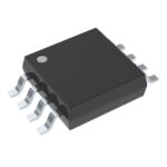 MAX22506EAUA+

The activity of extra discounts on wholesale prices is in full swing…
Please fill in your contact information and we will send you the latest wholesale price list.





