 ChipApex | Global Electronic Components Supplier

SEARCH
Search Product
Search Post
— IC芯片 | 连接器 | 传感器 | 被动器件 —
Search productSearch post
— IC芯片 | 连接器 | 传感器 | 被动器件 —
Consult the customer manager about the wholesale price.
consultation hotline:86-132-6715-2157
email:[email protected]
Contact the product manager for consultation. One-stop consultation is available.
Do you want a lower wholesale price? Please send us your inquiry and we will reply immediately.
The MAX241CWI is a +5V-powered, multichannel RS-232 transceiver from the MAX220–MAX249 family. It integrates four drivers and five receivers for full-duplex communication at data rates up to 120 kb/s. The device operates on a single +5V supply by utilizing internal charge-pump circuitry to generate ±10V internally. It features a shutdown mode that reduces power consumption significantly. The component is housed in a 28-pin Wide SOIC package and supports an operating temperature range of 0°C to +70°C.
Verify the specific suffix 'CWI' against the manufacturer's current ordering guide to confirm the package type and commercial temperature rating. Ensure the required external capacitors are included in the bill of materials, as the datasheet specifies their values for proper charge-pump operation.
Select this part when a single +5V supply is available but standard RS-232 voltage levels are required. Compare it against the MAX241ECWI if extended industrial temperature ranges or higher ESD protection ratings are necessary for the target environment.
This component belongs to the MAX220–MAX249 family of line drivers and receivers designed for EIA/TIA-232E and V.28/V.24 interfaces. The family offers various channel counts and package options to accommodate different board space constraints while maintaining compatibility with standard RS-232 signaling protocols.
The MAX241ECWI serves as a verified alternative within the same family, offering identical functionality with an extended temperature range. Other members of the MAX220–MAX249 series may be considered if channel counts differ, though pinouts must be verified for compatibility.
The device requires four external capacitors (C1 through C4) to support the internal charge-pump circuitry. Standard values are typically 1µF, though smaller values like 0.1µF may be used depending on specific load conditions.
When the shutdown pin is activated, the internal charge pumps cease operation. Consequently, the V+ pin falls to +5V and the V- pin falls to 0V, placing the transmitter outputs in a high-impedance state.
Yes, the receiver inputs are designed to accept signals from both TTL and CMOS logic families, ensuring broad compatibility with various microcontroller and processor interfaces.
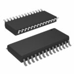 MAX241CWI

The activity of extra discounts on wholesale prices is in full swing…
Please fill in your contact information and we will send you the latest wholesale price list.





