 ChipApex | Global Electronic Components Supplier

SEARCH
Search Product
Search Post
— IC芯片 | 连接器 | 传感器 | 被动器件 —
Search productSearch post
— IC芯片 | 连接器 | 传感器 | 被动器件 —
Consult the customer manager about the wholesale price.
consultation hotline:86-132-6715-2157
email:[email protected]
Contact the product manager for consultation. One-stop consultation is available.
Do you want a lower wholesale price? Please send us your inquiry and we will reply immediately.
The MAX241EEAI+ is a single-supply RS-232 transceiver manufactured by Analog Devices Inc. It operates on a +5V supply and features four drivers and five receivers for full-duplex communication. The device supports data rates up to 120kbps with a typical propagation delay of 10µs. It includes an integrated charge pump requiring four 1µF external capacitors to generate ±10V levels. The component provides ±15kV ESD protection via the Human Body Model and operates within a temperature range of -40°C to +85°C. Supply current is typically 15mA, reducing to 1µA in shutdown mode.
Verify the specific suffix 'E' confirms the extended temperature range (-40°C to +85°C) and enhanced ESD protection compared to standard variants. Confirm the 'AI' suffix corresponds to the 28-pin SSOP package. Ensure the '+' designation indicates compliance with RoHS directives. Cross-reference the manufacturer part number with official distributor catalogs to confirm availability status and lead times.
Select this component when designing systems that require multiple transmitter and receiver channels on a single +5V rail. The MAX241EEAI+ is suitable for applications needing high ESD immunity on I/O lines. Verify that the required data rate does not exceed 120kbps under heavy capacitive loads. Consider the 28-pin SSOP footprint constraints during PCB layout planning.
This device belongs to the MAX202E–MAX213E family of RS-232 transceivers. It shares architectural similarities with the MAX232E but offers increased channel density with four drivers and five receivers. The 'E' variant distinguishes it from standard parts by providing ruggedized ESD protection structures suitable for notebook computers and industrial interfaces.
The MAX241EWI+ serves as a pin-compatible alternative in the wide SOIC-28 package. The MAX241EEWI+ offers the same electrical specifications in a narrow SOIC-28 package. Verify package dimensions and thermal characteristics when substituting these variants.
The EN (Enable) pin is active-low and puts receiver outputs into a high-impedance state. The SHDN (Shutdown) pin is active-high and disables the charge pumps and driver outputs to reduce power consumption.
Unused driver inputs have internal 400kΩ pull-up resistors to VCC. This forces the corresponding driver outputs low, preventing floating inputs and ensuring stable operation without external components.
The datasheet specifies four 1µF capacitors for the charge pump circuitry (C1–C4). Capacitor values up to 10µF can be used to improve performance if power is drawn from the V+ or V- rails.
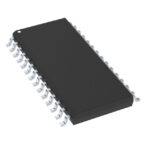 MAX241EEAI+

The activity of extra discounts on wholesale prices is in full swing…
Please fill in your contact information and we will send you the latest wholesale price list.





