 ChipApex | Global Electronic Components Supplier

SEARCH
Search Product
Search Post
— IC芯片 | 连接器 | 传感器 | 被动器件 —
Search productSearch post
— IC芯片 | 连接器 | 传感器 | 被动器件 —
Consult the customer manager about the wholesale price.
consultation hotline:86-132-6715-2157
email:[email protected]
Contact the product manager for consultation. One-stop consultation is available.
Do you want a lower wholesale price? Please send us your inquiry and we will reply immediately.
The MAX3054ASD+ is a ±80V fault-protected CAN transceiver designed for high-speed data rates up to 250kbps. It operates within an extended temperature range of -40°C to +125°C and utilizes a 14-pin SOIC package. The device supports full-duplex communication with a supply voltage range of 4.75V to 5.25V. Key electrical characteristics include a receiver hysteresis of 18mV, ensuring reliable signal detection in noisy environments. The component integrates current-limiting and thermal-protection circuits to safeguard the transmitter output stage against overcurrent faults and excessive junction temperatures.
Verify that the ordering suffix ASD+ corresponds to the lead-free and RoHS-compliant package variant as specified in the official datasheet. Confirm the manufacturer designation matches Analog Devices Inc., which acquired Maxim Integrated. Ensure the part number aligns with the 14-SOIC physical footprint and the specified -40°C to +125°C temperature grade before finalizing procurement orders.
Select the MAX3054ASD+ specifically for applications requiring data rates up to 250kbps. Choose this model over the MAX3055 or MAX3056 variants if higher speed is necessary, as those are optimized for 125kbps and 40kbps respectively. Ensure the design accommodates the 14-SOIC package dimensions and the required supply voltage range of 4.75V to 5.25V for proper operation.
The MAX3054 belongs to the MAX3054/MAX3055/MAX3056 family of ±80V fault-protected CAN transceivers manufactured by Analog Devices Inc. These devices serve as the interface between protocol controllers and the physical bus lines. The MAX3054 variant is distinguished by its optimization for high data rates, whereas sibling models target lower speed requirements with built-in slope control features for unshielded cable compatibility.
The MAX3054ASD+ is pin and functionally compatible with the TJA1054. Verify that any substitute component maintains the same ±80V fault protection rating and 250kbps data rate specification to ensure system integrity without redesigning the PCB layout.
The device detects various wiring failures such as shorts to battery, ground, or VCC, and open wires. Upon detection, it switches to single-wire mode to maintain communication and asserts the ERR pin low to indicate the fault condition.
The INH pin serves as an inhibit output used to deactivate an external voltage regulator. It goes high during wake-up requests or power-up to allow the regulator to shut down during sleep mode, thereby reducing overall power consumption.
Yes, during certain failure modes like CANH shorted to battery or CANL shorted to ground, the receiver switches to single-ended mode on the remaining functional bus line to preserve communication capability.
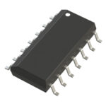 MAX3054ASD+

The activity of extra discounts on wholesale prices is in full swing…
Please fill in your contact information and we will send you the latest wholesale price list.





